PHT.301 Physics of Semiconductor Devices
|
|
PHT.301 Physics of Semiconductor Devices | |
|
|
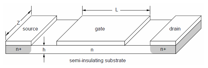
n-MESFET
The expression for the drain current of an n-channel MESFET is: \[ \begin{equation} I_{D}=I_p\left[\frac{V_D}{V_p}-\frac{2}{3}\left(\frac{V_{bi}-V_G+V_{D}}{V_p}\right)^\frac{3}{2}+\frac{2}{3}\left(\frac{V_{bi}-V_G}{V_p}\right)^\frac{3}{2}\right] \end{equation} \]Where the drain voltage $V_D$ and gate voltage $V_G$ are measured with respect to the source. The pinch-off voltage $V_P$ and pinch-off current $I_P$ are defined as, \[ \begin{equation} V_P=\frac{eN_Dh^2}{2\varepsilon_0\varepsilon_r}, \end{equation} \] \[ \begin{equation} I_p=\frac{e^2\mu_nN_D^2Zh^3}{2L\varepsilon_0\varepsilon_r}. \end{equation} \]For a Schottky junction, the built-in voltage is, \[ \begin{equation} eV_{bi}=\phi_b-k_BTln\left(\frac{N_c}{N_D}\left(\frac{T}{300}\right)^\frac{3}{2}\right) \end{equation} \]Where $\phi_b$ is the Schottky barrier height. The equation above for the drain current is only valid if the MESFET is in the linear regime where $V_{D}\le V_p-V_{bi}+V_G$. For larger drain voltages, the drain current saturates to, \[ \begin{equation} I_{D,sat}=I_p\left[\frac{1}{3}-\frac{V_{bi}-V_G}{V_p}+\frac{2}{3}\left(\frac{V_{bi}-V_G}{V_p}\right)^\frac{3}{2}\right]. \end{equation} \]
$V_{bi}=$ V; $I_p=$ mA; $V_p=$ V. |