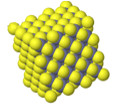
A small part of the crystal that can be repeated to form the entire crystal is called a unit cell.
Primitive unit cell
Conventional unit cell
Crystal
A primitive unit cell is the smallest pattern that can be repeated to form the whole crystal. For crystals with cubic symmetry, the conventional unit cell is the smallest cube that can be repeated to form the whole crystal.
Devices such as solid state transistors, lasers, solar cells, and light emitting diodes are often made from large single crystals that are cut into thin wafers. As light, sound, or electrons move through a crystal, they propagate as waves and diffract from the lattice of atoms. A consequence of the diffraction of electron waves is that electrons of certain energies cannot move through the crystal. A range of forbidden electron energies is called an energy band gap.
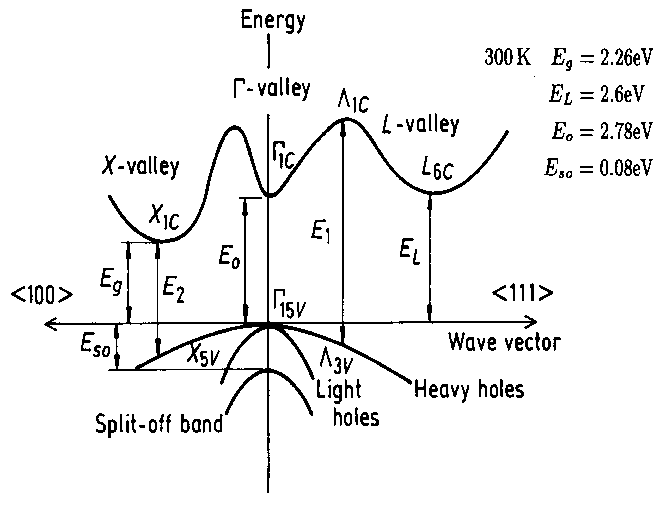
Below, simplified band diagrams can be displayed for some semiconductors. The electrons in the conduction band are primarily located at the minimum of the conduction band and the holes in the valence band are concentrated at the maximum of the valence band. The electrons are thermally excited up to about $k_BT$ above the conduction band minimum and the holes are excited to about $k_BT$ below the valence band maximum.
Simplified band structure of GaP. From NSM Archive.
Know that most of the important metals and semiconductors in electronics form crystals where the atoms arrange in a periodic pattern. An important exception is the insulating material silicon dioxide. The atoms have a random order in SiO2.
You should how to specify directions in a crystal with Miller indicies.
Electrons and photons move like waves but exchange energy and momentum like particles. The energy is $E$ is related to the frequency $f$ of the wave by Planck's constant $h$, $E=hf$. The momentum of an electron or a photon is given by the de Broglie relation $\vec{p} = \hbar\vec{k}$ where $\vec{p}$ is the momentum, $\hbar=\frac{h}{2\pi}$ is the reduced Planck's constant and $\vec{k}$ is the wavevector. The wavevector points in the direction that the wave is moving and is related to the wavelength of the wave by $ \lambda = \frac{2\pi}{|\vec{k}|}$.
For photons the relationship between the energy and the wavevector is $E=\hbar c |\vec{k}|$. This yields the standard relationship between frequency and wavelength for a light wave $f=\frac{c}{\lambda}$.
For electrons, the relationship between the energy and the wavevector is called the band structure and it depends on the material that the electrons are moving in. There are certain ranges of energies (called bands) where there are propagating electron solutions and other ranges of energies (called band gaps) where there are no electron solutions. Metals have a partially filled band while in semiconductors or insulators, there is a band gap that separates a valence band that is occupied by electrons from a conduction band which is empty. Some examples of band structures are GaAs, GaN, GaP, Ge, InAs, 6H SiC, V
By looking at the band structure or the density of states, you should be able to say if a material is a metal, a semiconductor, or an insulator.