PHT.301 Physics of Semiconductor Devices
|
|
PHT.301 Physics of Semiconductor Devices | |
|
|
Extrinsic semiconductorsIn the section on intrinsic semiconductors we found that the conductivity of an intrinsic semiconductor depends exponentially on temperature and that at room temperature intrinsic semiconductors are rather poor conductors. It is possible to dope semiconductors with impurity atoms that improve the conductivity dramatically and makes the conductivity nearly constant as a function of temperature near room temperature. Doped semiconductors are called extrinsic semiconductors. Reading: Singh 2.6 - 2.9 or Thuselt 2.3
Additional material
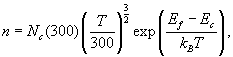
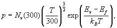
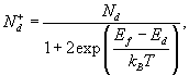
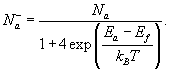
The donor energies are the differences of the donor levels Ed to the bottom of the conduction band Ec. The acceptor energies are the differences of the acceptor levels Ea to the top of the valence band Ev. Doped semiconductorsFor a doped semiconductor, the density of electrons in the conduction band is,
the density of holes in the valence band is,
the density of ionized donors is,
and the density of ionized acceptors is,
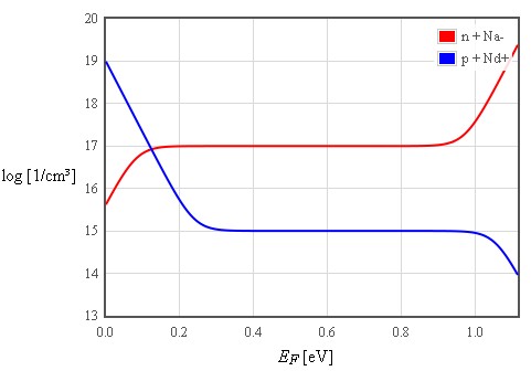
The factor of 4 is valid in the formula for the acceptors if the semiconductor has a light hole and a heavy hole band as Si and Ge do. The four quantities n, p, Nd, and Na can only be determined if the Fermi energy, Ef, is known. Typically, Ef must first be determined from the charge neutrality condition, n + Na- = p + Nd+. The Fermi energy can be found by solving the charge neutrality condition numerically. One way to do this is to program the formulas for n, p, Nd+, and Na- in a spreadsheet. Then choose a temperature and calculate n, p, Nd+, Na- for every value of the Fermi energy between Ev and Ec. For one of these Ef values, the charge neutrality condition will be satisfied. When n + Na- and , p + Nd+ are ploted as a function of EF, the Fermi energy is where the two lines cross. A plot like the one below can be generated by pressing the button below the plot.
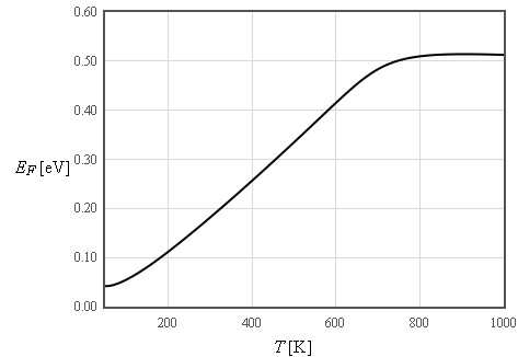
The Fermi energy can be calculated as a function of temperature by determining where n + Na- = p + Nd+ for every temperature. A plot like the one below can be generated by pressing the button below the plot.
Normally it is not necessary to determine Ef numerically and the following approximation is sufficient. n-type Nd > Na: n = Nd - Na p-type Na > Nd: p = Na - Nd |