PHT.301 Physics of Semiconductor Devices
|
|
PHT.301 Physics of Semiconductor Devices | |
|
|
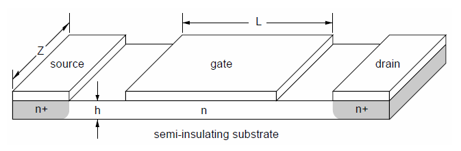
MESFET Gradual Channel ApproximationThe description of a MESFET in the gradual channel approximation is almost the same as for a JFET. The difference is how the built-in voltage $V_{bi}$ is calculated. Consider an $n$-channel MESFET.
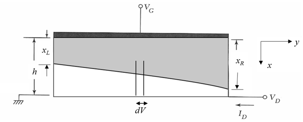
A MESFET consists of a semiconducting channel contacted by two ohmic contacts. The metal gate forms a Schottky contact above the channel. The current in the channel flows between the depletion layer of the Schottky diode and a semi-insulating substrate. When the Schottky contact is reverse biased, the depletion width expands and the channel becomes narrower. The thickness of the conducting channel is $h-x_n(y)$ where $h$ is the thickness of the $n$-doped channel and $x_n(y)$ is the depletion width that depends on the position $y$ along the channel. In the figure below, the gray region of the channel is depleted.
A constant current $I_D$ flows from the drain to the source. The voltage drop across a short section of the channel is $dV = I_DR$, where $R$ is the resistance of this short section. Ohm's law states, \[\begin{equation} R = \frac{\rho dy}{(h-x_n(y))Z}. \end{equation}\]For an $n$-doped extrinsic semiconductor, the resistivity is $\rho=1/(e\mu_nN_D)$ where $-e$ is the charge of an electron, $\mu_n$ is the electron mobility, and $N_D$ is the donor concentration. This can be combined to yield, \[\begin{equation} I_Ddy = e\mu_nN_DZ(h-x_n(y))dV \end{equation}\]The formula for the depletion width of a Schottky diode is the same as for a one-sided $pn$-junction, \[\begin{equation} x_n = \sqrt{\frac{2\epsilon_r\epsilon_0(V_{bi}-V)}{eN_D}}, \end{equation}\]where $V_{bi}$ is the built-in voltage and $V$ is the forward bias voltage across the Schottky diode. In the case of an n-MESFET, a positive voltage on the gate forward biases the diode and a positive voltage on the drain reverse biases the diode so the depletion with is, \[\begin{equation} x_n(y) = \sqrt{\frac{2\epsilon_r\epsilon_0(V_{bi}+V(y)-V_G)}{eN_D}}, \end{equation}\]where $V(y)$ is the potential along the channel. Differentiating this expression, we find, \[\begin{equation} \frac{dx_n(y)}{dV} = \frac{1}{2\sqrt{\frac{2\epsilon_r\epsilon_0(V_{bi}+V(y)-V_G)}{eN_D}}}\frac{2\epsilon_r\epsilon_0}{eN_D}=\frac{\epsilon_r\epsilon_0}{eN_Dx_n(y)}. \end{equation}\]Thus, \[\begin{equation} dV =\frac{eN_Dx_n}{\epsilon_r\epsilon_0}dx_n. \end{equation}\] Substituting this into Eq. 2 yields a first-order differential equation that can be solved for the depletion width as a function of position along the channel. \[\begin{equation} I_Ddy = \frac{e^2\mu_nN_D^2Z}{\epsilon_r\epsilon_0}(h-x_n)x_ndx_n. \end{equation}\]Integrating from source to drain, \[\begin{equation} I_D\int\limits_0^L dy = \frac{e^2\mu_nN_D^2Z}{\epsilon_r\epsilon_0}\int\limits_{x_L}^{x_R}(h-x_n)x_ndx_n. \end{equation}\]The depletion width at the source is $x_L$, the depletion width at the drain is $x_R$. \[\begin{equation} \frac{I_D\epsilon_r\epsilon_0L}{e^2\mu_nN_D^2Z}= \frac{hx_R^2}{2} -\frac{x_R^3}{3}-\frac{hx_L^2}{2} +\frac{x_L^3}{3}. \end{equation}\]Using the expressions for the depletion widths at the source and the drain and the definition of the pinch-off voltage $V_p$, \[\begin{equation} x_L = \sqrt{\frac{2\epsilon_r\epsilon_0(V_{bi}-V_G)}{eN_D}},\qquad x_L = \sqrt{\frac{2\epsilon_r\epsilon_0(V_{bi}+V_D-V_G)}{eN_D}},\qquad h = \sqrt{\frac{2\epsilon_r\epsilon_0V_p}{eN_D}}, \end{equation}\]the drain current in the linear regime can be expressed in terms of the gate voltage and drain voltage, \[ \begin{equation} \boxed{I_D=I_p\left[\frac{V_D}{V_p}-\frac{2}{3}\left(\frac{V_{bi}+V_D-V_G}{V_p}\right)^{3/2}+\frac{2}{3}\left(\frac{V_{bi}-V_G}{V_p}\right)^{3/2}\right].} \end{equation} \]Here, \begin{align} I_p =\frac{\mu_n {N_D}^2 Z e^2 h^3}{2L\epsilon_r\epsilon_0}, \qquad V_p =\frac{e {N_D} h^2}{2 \epsilon_r\epsilon_0}, \qquad eV_{bi} =\phi_b - k_B T \ln \left(\frac{N_c}{N_D}\left(\frac{T}{300}\right)^{3/2}\right). \end{align}Here $\phi_b$ is the Schottky barrier height and $N_c$ is the effective density of states of the conduction band at 300 K. Eq. 11 for the drain current is valid in the linear regime before the channel is pinched-off. After pinch-off, the MESFET is in the saturation regime and the current is, \[ \begin{equation} I_{D,sat}=I_p\left[\frac{1}{3}-\frac{V_{bi}-V_G}{V_p}+\frac{2}{3}\left(\frac{V_{bi}-V_G}{V_p}\right)^{3/2}\right]. \end{equation} \]This derivation assumed that the Schottky diode is reverse-biased. For an n-channel MESFET, $V_G$ < 0 and $V_D$ > 0 in this regime. The gray area of the plot below shows the part of the channel that is depleted.
$V_{bi}=$ V; $I_p=$ mA; $V_p=$ V $I_d=$ mA $x_L=$ μm $x_R=$ μm. |