
PHT.301 Physics of Semiconductor Devices
|
|
PHT.301 Physics of Semiconductor Devices | |
|
|
Tunnel diodes / Esaki diodes
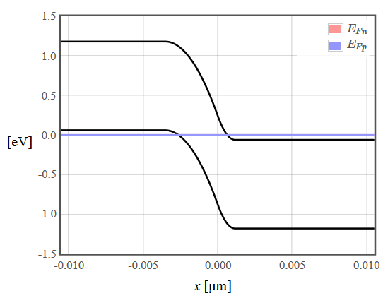
A tunnel diode (also called an Esaki diode) is a pn-diode where both sides have been degenerately doped so that the Fermi energy is in the conduction band on the n-side and it is in the valence band on the p-side. The heavy doping results in a narrow depletion width that electrons can tunnel through. At zero bias, the Fermi energy is the same on both sides, and the current is zero.
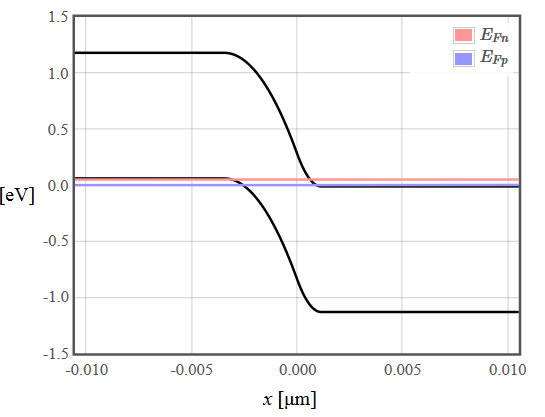
As a forward voltage is applied, the quasi-Fermi energies of electrons and holes separate and all of the states between the two quasi-Fermi energies are occupied on the n-side and empty on the p-side so electrons can tunnel across the junction.
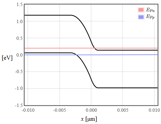
Initially, the number of states that can participate in tunneling increases as the bias voltage increases, so the current increases with the bias voltage. However, at a certain forward bias voltage, the occupied states on the n-side move higher in energy than the empty states on the p-side, and the tunnel current decreases.
There is a range of forward bias voltage where negative differential resistance is observed until the voltage is high enough that the standard diffusion current mechanism takes over and the current increases again.
|

