
PHT.301 Physics of Semiconductor Devices
|
|
PHT.301 Physics of Semiconductor Devices | |
|
|
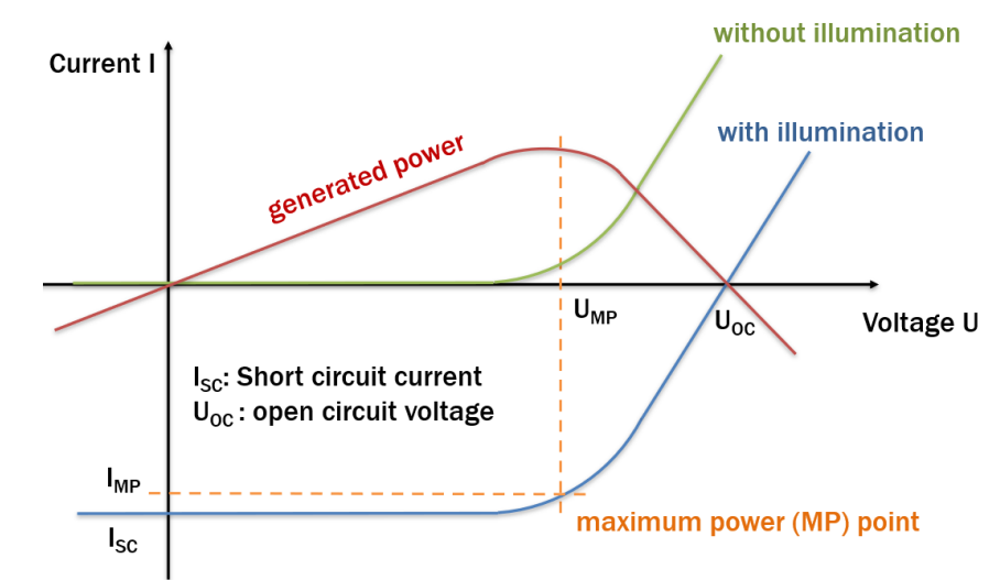
Solar CellsA solar cell is a large area pn-junction. Typically, the light enters through a thin, heavily-doped n layer that is above a more lightly doped p layer. A depletion layer forms between the n and p layers with an electric field that points down towards p. If a photon that enters through the n-layer has enough energy to generate an electron-hole pair in the depletion layer, this electron-hole pair will be separated by pushing the electron towards the n-layer and the hole towards the p-layer. The charge separation puts more positive charge on the p-side and more negative charge on the n-side. This forward biases the pn-junction. Nevertheless, current can be extracted from the device if it is connected to a load with a lower impedance than a forward-biased diode. Often, silver lines are screen printed on the top of the solar cell to make an electrical connection to the n-side, and a p+ layer is put under the lightly doped p-region so that a tunnel contact can be made to the p+ layer on the p-side.
Photons striking the surface of the solar cell will be partially reflected and partially transmitted into the semiconductor. The reflected light can be minimized with antireflective coatings or by roughening the surface. Once the light enters the semiconductor, absorption takes place following the Beer-Lambert law, $I=I_0\exp(-\alpha x)$. Here, $I$ is the intensity of the light, $I_0$ is the intensity at the surface, $\alpha$ is the absorption coefficient, and $x$ is the distance the light has traveled into the semiconductor. The upper n-layer should be thin enough that few photons are absorbed in that layer. Any electron-hole pair generated in the heavily doped n-layer will likely quickly recombine because of the high concentration of electrons. For this reason, the n-layer is kept thin. Since this thin layer must also carry the current, it is typically doped n-type since the electrons usually have the higher mobility. The incoming photons must have enough energy to promote an electron from the valence band to the conduction band. For an indirect bandgap semiconductor like silicon, the photons need more energy than the indirect band gap energy. The electrons therefore enter the conduction band at an energy higher than the conduction band minimum, and through electron-electron interactions, the electrons will fall quickly to the bottom of the conduction band, and the holes will fall to the top of the valence band. The result is that only the band gap energy can be extracted for each photon that creates an electron-hole pair, regardless of the photon energy. If the photon is absorbed in the lightly doped p-layer below the depletion layer, the electron and hole that are generated will diffuse around. If the electron reaches the depleted region before it recombines, it will be pushed to the n-side.
|
