A Light Emitting Diode (LED) consists of a pn-diode in a semiconductor with a direct bandgap. When the diode is forward biased, the electrons and the holes are pushed towards the junction where they recombine. The photons that are emitted have the energy of the band gap, $E_g = \frac{hc}{\lambda}$. The slider below lets you select a wavelength. The corresponding bandgap to this wavelength is calculated and the approximate color is shown. For some bandgap energies, the composition of a direct bandgap semiconductor that will emit this wavelength is shown.
Below, simplified band diagrams can be displayed for some semiconductors. The electrons in the conduction band are primarily located at the minimum of the conduction band and the holes in the valence band are concentrated at the maximum of the valence band. The electrons are thermally excited up to about $k_BT$ above the conduction band minimum and the holes are excited to about $k_BT$ below the valence band maximum. When the electrons and holes recombine, this results in photon energies approximately in the range $E_g \pm k_BT$.
Simplified band structure of GaP. From NSM Archive.
Direct:
Indirect:
When an electron makes a transition from the conduction band to the valence band, energy and momentum must be conserved.
$$\text{conservation of energy}\qquad E_c(\vec{k}_c) - E_v(\vec{k}_v) = E_g = hf_{\text{photon}}$$
$$\text{conservation of momentum}\qquad \hbar\vec{k}_c - \hbar\vec{k}_v= \hbar \vec{k}_{\text{photon}}$$
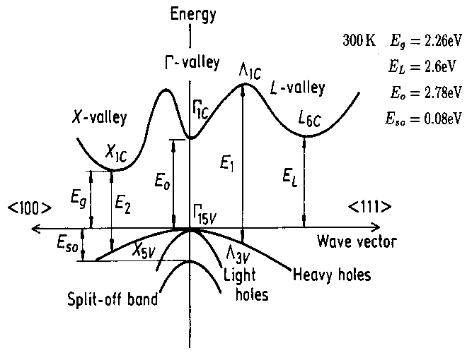
The momentum of a visible photon $\hbar \vec{k}_{\text{photon}}$ is much smaller than the momentum of an electron in a $\vec{k}$-state on the Brillouin zone boundary. Consequently, an electron makes a virtually vertical transition in these band diagrams from the conduction band to the valence band when it emits a photon. Therefore, semiconductors used in light-emitting diodes must have a direct band gap so that the electrons in the conduction band can fall directly down into the holes in the valence band. Forward-biased diodes of indirect bandgap semiconductors typically emit phonons instead of photons. The phonons can absorb the momentum needed when the electrons fall from a $\vec{k}$ state in the conduction band to a different $\vec{k}$ state in the valence band.
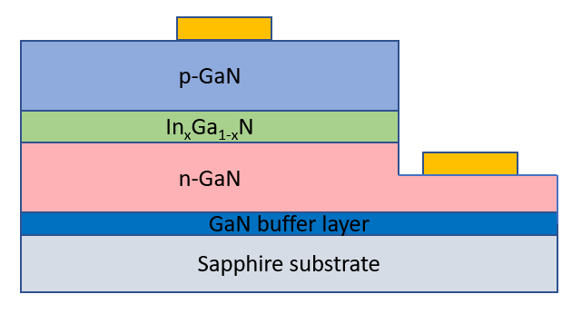
Light-emitting diodes are usually made of semiconductors that are grown epitaxially. A single crystal is grown in layers where the materials composition (doping and bandgap) is changed during growth. The figure below shows the typical structure of the semiconductor in a LED. After the layered material is grown, it is selectively etched back and metal contacts are made to the n- and p-sides of the diode.
In this example, light is emitted in the InxGa1-xN layer. The bandgap of this layer determines the color of the light emitted. The surrounding layers of GaN and Sapphire have larger bandgaps than the InxGa1-xN layer so the photons will not be absorbed in the surrounding material.
Coupling the light out
Typically the semiconductor in an LED is embedded in a (colored) clear epoxy. The photons are emitted by spontaneous emission in random directions inside the semiconductor. Some of the photons generated in a LED are reabsorbed or are reflected at the semiconductor-epoxy interface due to total internal reflection so that only a fraction of the light couples out of the device. The index of refraction of a semiconductor is usually higher than the index of refraction of the epoxy so light rays are refracted at the interface between the materials according to Snell's law, $n_s\sin\theta_s = n_e\sin\theta_e$. Here $n_s$ and $n_e$ are the indices of refraction in the semiconductor (s) and the epoxy (e). $\theta_s$ and $\theta_e$ are the angles the light rays make to the normal of the interface. The simulation below shows what happens when light rays leave a point source in the semiconducting material (blue) and they refract at the interface to the epoxy (green). For large angles $\theta_s$, there is no solution to $n_s\sin\theta_s = n_e\sin\theta_e$ and the light rays are reflected at the interface.
Approaches to more efficiently couple the light out of the semiconductor are to use an encapsulation with a higher index of refraction or to roughen the interface. A good reference for Light Extraction Efficiency (LEE) is Invention, development, and status of the blue light-emitting diode by Daniel Feezell and Shuji Nakamura.
The structure of a LED A typical LED is shown in Fig. 1. The semiconducting die is a few hundred microns on a side. It is much smaller than 5 mm lens. The semiconductor chip is attached by a conducting adhesive in a reflective cavity in the anvil. A 25 μm gold wire is bonded between the post and the top of the semiconductor. An epoxy resin lens in molded around the semiconductor.
Below is a section through an x-ray computed tomography image of the semiconducting die in the reflective cavity. The rectangular semiconducting die has a width of 370 μm and is 170 μm high. It is attached to the reflective cavity by conducting adhesive and a gold wire is bonded to the top of the die.


.svg)