Experimental Laboratory Exercises
|
|
Experimental Laboratory Exercises | |
|
|
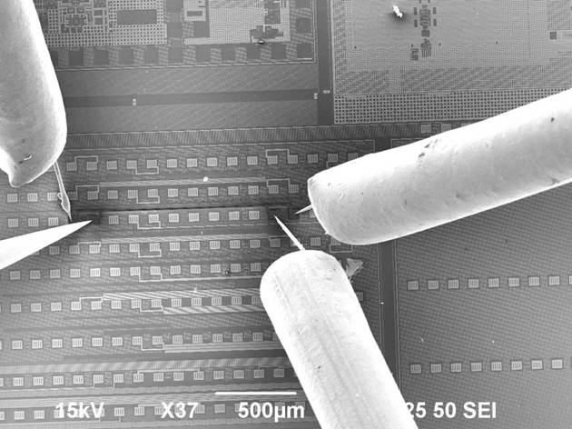
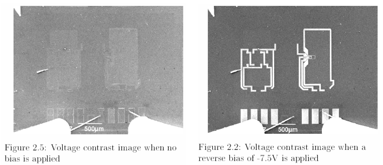
Voltage contrastIf a region of the specimen is given a positive bias, fewer secondary electrons will be emitted. By comparing images before and after a voltage has been applied it is sometimes possible to see where the voltage drops in a sample by observing the change in grayscale.
A four-point measurement of a wire in an integrated circuit. The wires that are not connected charge to a negative voltage due to the electron beam. The connected wire is black since it does not charge.
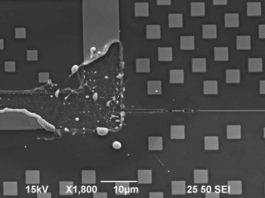
The wire fused at 20 mA.
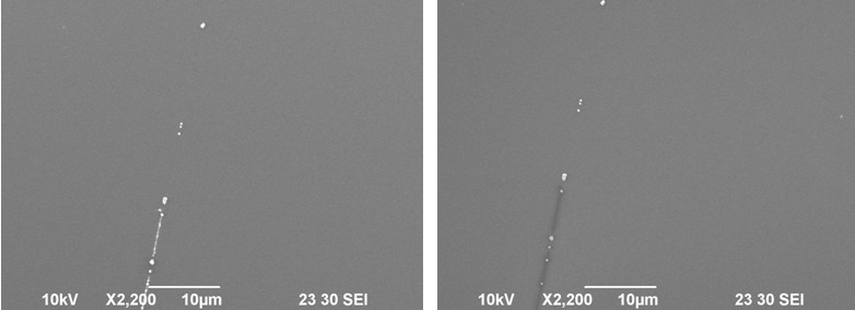
These images show a carbon nanotube that has been decorated with small gold clusters. The tube is broken in the middle of the picture. On the left, a negative voltage is applied to the nanotube and it is bright in the picture until the point where it is broken. On the right, a positive voltage is applied to the nanotube and it is dark until the point where it is broken.
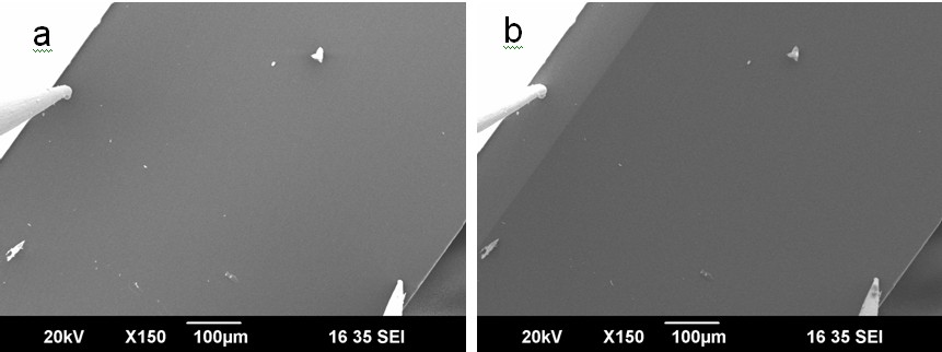
The two SEM images above are of a cross section of a silicon substrate that has a pn junction in it. When the junction is reverse biased (b), there is a change in color at the abrupt change in voltage at the junction.
|