Experimental Laboratory Exercises
|
|
Experimental Laboratory Exercises | |
|
|
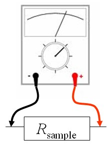
Four point resistivity measurementsWhen resistance is measured with a simple ohmmeter, the resistance of the cables leading to the sample and any resistance at the contacts is measured as well as the resistance of the sample.
The contact resistances can be a serious problem when electrical contact is made using the micromanipulators since the contact area is very small.
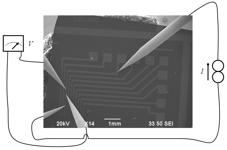
To overcome the problem of the contact resistances, a four probe configuration can be used.
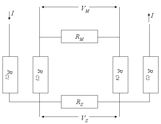
A current is passed through the two outer contacts while the voltage is measured between the two inner contacts. The equivalent circuit for a four point measurement is,
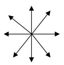
Current flows into the sample at contact 1 and comes out of the sample at contact 2. Here RCi is the cable resistance and contact resistance of contact i. Usually the contact resistance dominates over the cable resistance. RS is the sample resistance and RM is the equivalent resistance of the voltmeter. VS is the voltage across the sample and VM is the voltage measured by the voltmeter. Four point measurements on a thin filmWhen a current contact is placed on a thin conducting film with a uniform resistivity ρ and a current I is injected into this contact, the current spreads radially and the current density around the contact is,
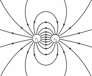
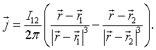
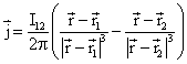
Here t is the thickness of the film. If two current contacts are placed on a thin film and a current I12 is injected into the surface at position r1 while it is extracted from position r2, then the currents just add and the folloing dipole pattern is produced. The thin film approximation is valid if the distance between the contacts is much larger than the thickness of the film.
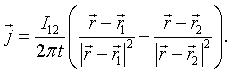
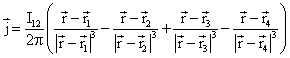
In this case the current density is given by,
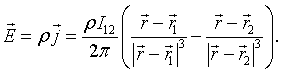
The electric field is the resistivity ρ times the current density,
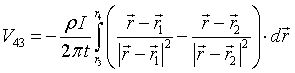
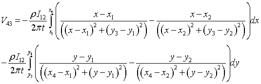
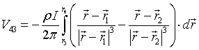
The voltage between position r3 and position r4 on the surface is minus the integral of the electric field from one position to the other. The potential at r4 measured with respect to the potential at r3 is,
The voltage is independent of the path that is taken. We choose to integrate first in the x-direction and then in the y-direction.
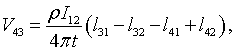
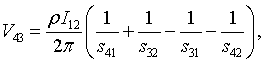
After performing the integration, the following expression for the voltage is found,
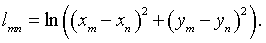
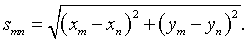
where
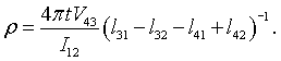
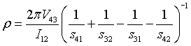
The expression for the resistivity is,
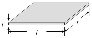
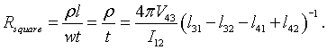
Sometimes the thickness of the conducting film is not known accurately. In this case the sheet resistance, Rsquare, is given. The sheet resistance is the resistance of a square of the film.
The size of the square does not matter because l = w and these factors cancel out of the expression for Rsquare.
If the thickness t is not known, leave the textbox for t blank and only the sheet resistance will be calculated. The formula for the sheet resistance takes a simple form if the four contacts are in a straight line and equally spaced. If the current is driven between the inner contacts and the voltage is measured between the outer countacts (or the current is driven between the outer contacts and the voltage is measured between the inner contacts), the sheet resistance is, $$R_{\text{square}}=\frac{\pi V}{\ln (2) I}\,\,\Omega /\square.$$Four point measurements on a thick filmIf a current contact is placed on a flat surface of some material with a uniform resistivity ρ and a current I is injected into this current contact, the current spreads radially and the current density below the contact is,
If two current contacts are placed on a flat surface and a current I12 is injected into the surface at position r1 while it is extracted from position r2, then the current density is given by,
The thick film approximation is valid when the distance between the contacts is much smaller than the thickness of the film. The electric field is the resistivity times the current density,
The voltage between position r3 and position r4 on the surface is minus the integral of the electric field from one position to the other. The potential at r4 measured with respect to the potential at r3 is,
On the surface, z = 0. The voltage is independent of the path that is taken. We choose to integrate first in the x-direction and then in the y-direction.
After performing the integration, the following expression for the voltage is found,
where
The expression for the resistivity is,
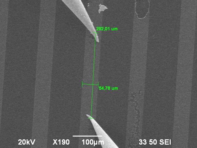
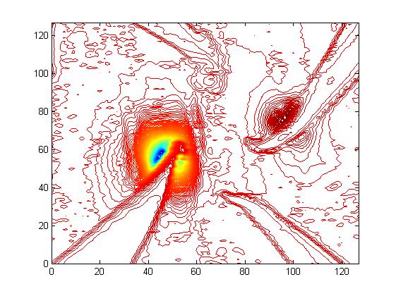
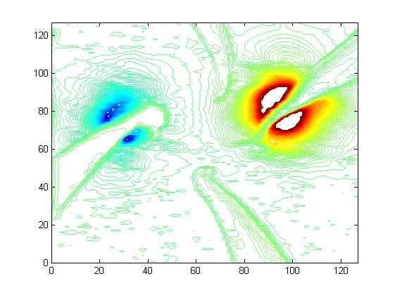
The formula for the resistivity takes a simple form if the four contacts are in a straight line and equally spaced a distance $a$ apart. If the current is driven between the inner contacts and the voltage is measured between the outer countacts, the resistivity is, $$\rho=\frac{2\pi aV}{ I}\,\,\Omega\text{ m}.$$This formula holds if the four contacts are far from the edges of the film and the film thickness $t$ is much larger than the spacing between the contacts, $t > > a$. If the four contacts are equally four contacts are in a straight line and and far from the edges but $t$ is on the order of the spacing between the contacts, $$\rho=\frac{2\pi V}{ I}\left(\frac{1}{a}+\frac{2}{\sqrt{a^2+4t^2}}-\frac{1}{\sqrt{a^2+t^2}}\right)^{-1}\,\,\Omega\text{ m}.$$Sometimes the tips have been bent and it is hard to know where they are making electrical contact. If the sample that is being measured is a semiconductor, the Schottky contacts can be imaged with EBIC as illustrated in the figures below.
Four point measurements on a thick film with edge-boundary conditionA current contact is placed on a flat surface of some material with a uniform resistivity ρ. When a current I is injected into this current contact, the current spreads radially and the current density below the contact is,
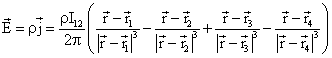
If two current sources are placed on a flat surface and a current I12 is injected into the surface at position r1 while it is extracted from position r2, then the current density is given by,
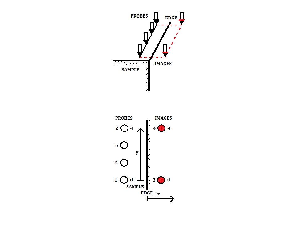
If the contacts are close to an edge of the sample certain boundary conditions have to be taken into account. One way to achieve this is to add two additional image current sources. These sources are mirror images of the "real" current sources with respect to the sample edge (see images above).
In this case there are two extra factors in the equation for the current density.
The electric field is the resistivity times the current density,
The voltage between position r5 and position r6 on the surface is minus the integral of the electric field from one position to the other. The potential at r6 measured with respect to the potential at r5 is,
On the surface, z = 0. The voltage is independent of the path that is taken. We choose to integrate first in the x-direction and then in the y-direction.
After performing the integration, the following expression for the voltage is found,
where
The expression for the resistivity is,
L. B. Valdes, Resistivity Measurements on Germanium for Transistors, Proceedings of the IRE, vol. 42, p. 420 (1954). |