Experimental Laboratory Exercises
|
|
Experimental Laboratory Exercises | |
|
|
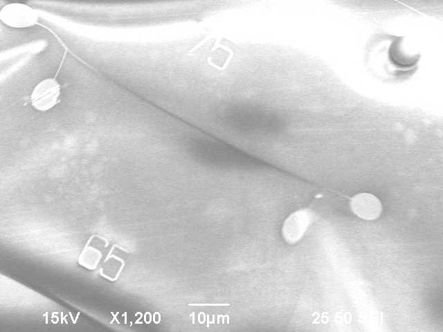
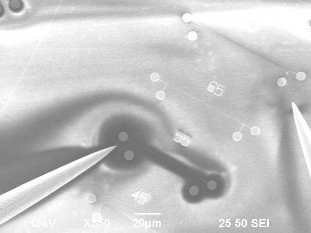
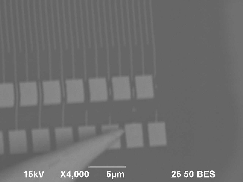
Electrostatic chargingNonconducting samples have a problem with charging. If the charge from the electron beam strikes a nonconducting surface and cannot flow away, the charge on the surface deflects the electron beam and it become impossible to form a good image. Typically the screen turns white when there is charging. Working at low resolution and low acceleration voltage (1 kV) helps to reduce the effects of charging. Putting a conducting tip on the surface allows you to focus on a small area around the tip.
By touching a grounded probe tip to the glass, the charge can be drawn away in an are around the tip and it is possible to get a clear image.
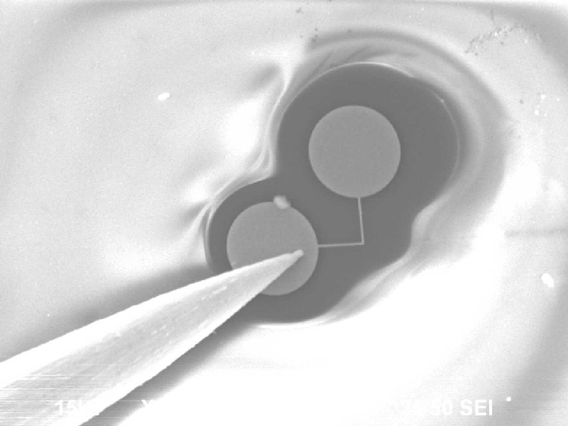
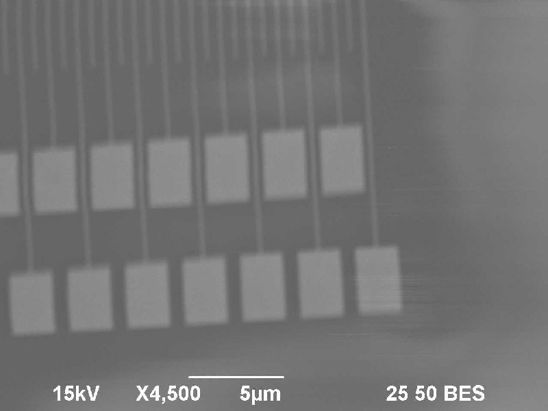
The backscatter detector has less trouble with charging than the secondary electron detector. Below images taken with the backscatter detector before and after a tip has been contacted to a gold line. The discharge of the charge when the tip came in contact with the gold lines caused the lines to fuse.
|