Experimental Laboratory Exercises
|
|
Experimental Laboratory Exercises | |
|
|
Electrical contactsWhen a sharp metal tip approaches a conducting surface, a tunnel current is first observed when the tip is a few angstroms from the surface. Often there is a nonconducting oxide layer on a conducting surface and the electrons tunnel through this insulating layer when the tip comes into contact with the surface. If the tip is pressed through the oxide, a metal-metal contact is made. Few atom contacts have been studied extensively. [Agraït] They exhibit steps in the conductance in units of the conductance quantum 2e²/h and they can carry very high current densities. One dimensional chains of gold atoms have been observed to carry current densities on the order of 1011 A/cm² [Yanson]. These few atom contacts are typically unstable; the resistance fluctuates continuously. If the tip is pushed harder so that a few square nanometers of metal come into contact, then a Sharvin contact is formed. [Sharvin] A Sharvin contact has a diameter smaller than the electron mean free path. The electrons travel ballistically through the contact region and the contact resistance is given by R = (h/2e²)(2/kFa)². Here kF is the Fermi wave number and a is the radius of the contact. If the tip is pressed harder against the surface so that the size of the contact is greater than the electron mean free path, the transport through the contact can be treated classically (a Holm contact) and the contact resistance is R = (ρ1+ρ2)/4a. [Holm] Here ρ1 and ρ2 are the resistivities of the tip and the conducting surface. If an electrical contact is made by pressing two metal plates together, the current does not flow uniformly. It is concentrated at many tiny spots where the two metals make intimate contact. There can be contributions to the total current due to tunneling, Sharvin contacts and Holm contacts but the Holm contacts have the lowest resistance and will carry the most current. Heating at a contact
Here T is the temperature and L = 2.44 × 10⁻⁸ V²/K² is the Lorentz number. Under these assumptions, the relation between the applied voltage V and the maximum temperature at the center of the contact Tm is, [Holm]
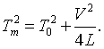
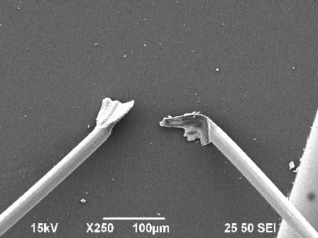
Here T0 is the temperature of the leads far away from the contact. Fairly modest applied voltages can cause the metal to melt at the constriction. The melting voltages for some materials are: Al = 0.3 V, Ni = 0.16 V, Cu = 0.43 V, Ag = 0.37 V, Sn = 0.13 V, Au = 0.43 V, W = 1.1 V, Pt = 0.65 V. [Slade] Experiments Small contacts can be subjected to very high electric fields and current densities. High electric fields can eventually lead to dielectric breakdown. Often this results in the contact resistance changing by a few orders of magnitude. Sometimes the probe tip is melted to the sample and the resistance becomes much lower and sometimes material is ablated away and all electrical contact is lost. High current densities (~ 1MA/mm²) cause local heating which leads to surface diffusion or bulk diffusion of the atoms at the contact as well at thermal expansion of the tips. Both of these effects make the contact resistance unstable. Mechanical vibrations of the building and piezo creep of the manipulators cause the probe tips to move and make the contacts unstable. Sometimes chemical reactions take place at the tips. Even in vacuum, there is a thin layer of water on the sample. If the tip and the sample are different materials, an electrochemical cell is formed and applying a voltage between the tip and the sample can etch or oxidize the sample. Copper - Tin contacts
When the wires are first put in contact, a resistance of a few kΩ is measured. This resistance stays constant as the current is increased until at few mA are flowing. The resistance then increases a few orders of magnitude. At a bias voltage of about 1 V the resistance suddenly drops to 20 Ohms. We have put 300 mA through such contacts. If the current is returned to zero and swept slowly again, the resistance is first low and then it gradually increases. At a voltage of about 1 V, there is a sudden transition to low resistance again. The wires are never strongly bonded together. When they are separated it is often not possible to detect where the point of contact was using the SEM. Some properties of Cu-Sn intermetallic compounds can be found in R. J. Fields and S. R. Low, PHYSICAL AND MECHANICAL PROPERTIES OF INTERMETALLIC COMPOUNDS COMMONLY FOUND IN SOLDER JOINTS Electromigration
The article that describes this movie is: In situ imaging of electromigration-induced nanogap formation by transmission electron microscopy Corrosion
A closer look at the tip reveals bubbles appearing at the tip where the cutting took place. Even a film that appears dry has a thin layer of water on it. The water and the applied voltage allowed the electrochemical removal of the chrome film. It appears that after the film is etched, the film gets thinner and the current density gets higher until the remaining film evaporates due to the high current density. Flashes can be seen in the first video where the edge of the cut turn white. This is due to heating by the current.
Below a chrome line in air changes color as a current is passed through it. This is presumably due to the oxidation of the chrome cause by current induced heating.
Thermal expansion Welding tips together Electrical forming
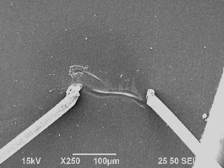
Tips sharpened by the focused ion beam
[Agraït] Nicolas Agraït, Alfredo Levy Yeyati, Jan M. van Ruitenbeek, Quantum properties of atomic-sized conductors, Physics Reports 377 p. 81 - 279 (2003). |