
Experimental Laboratory Exercises
|
|
Experimental Laboratory Exercises | |
|
|
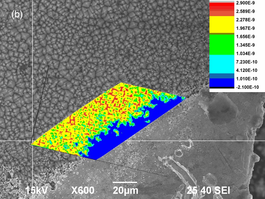
Electron Beam Induced Current (EBIC)Electron Beam Induced Current (EBIC) is a technique for measuring currents that flow in a semiconductor that is exposed to an electron beam. When the electron beam strikes a semiconductor, electron-hole pairs are created. If these pairs diffuse into a region with a built-in electric field, the electrons and holes will be separated and a current will flow. This is similar to how a solar cell works except that the electron-hole pairs are generated by an electron beam instead of light. Figure 1 shows a secondary electron image of a polycrystalline silicon solar cell. This is not a high quality solar cell. The electron beam was slowly scanned over a region of the solar cell and the current that was generated by the solar cell was measured. This current is displayed in color. The measured EBIC current was small when the beam fell on the metal contact but was larger when it fell on the active region of the solar cell. Within the active region of the solar cell there are large variations in the current. This is due to a variation in the density of defects which cause the electron-hole pairs to recombine before they are separated by the built-in electric field.
EBIC images can also be made of organic solar cells. Because the electron beam damages organic material, the EBIC measurement must be performed quickly before the organic material degrades.
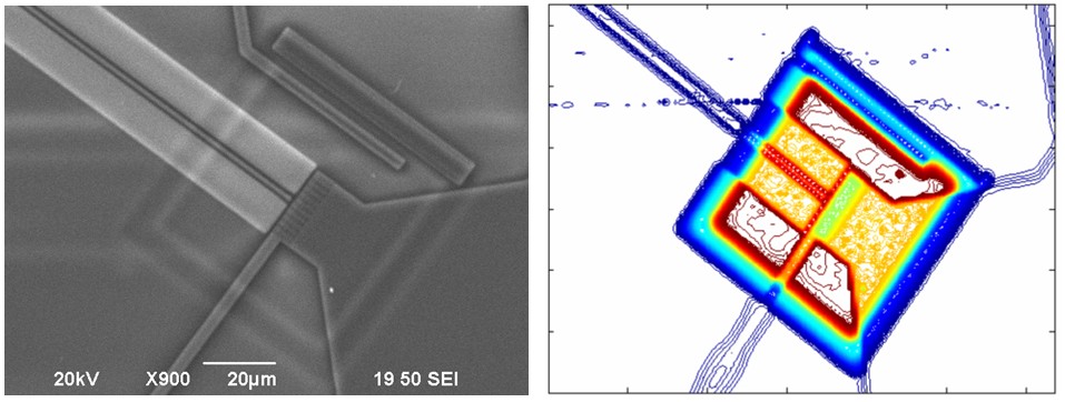
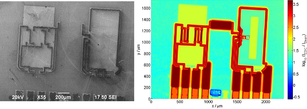
Integrated circuits contain many pn-junctions and Schottky contacts that act like solar cells. When they are irradiated by the electron beam, electron-hole pairs are produced and these generate an EBIC current. EBIC images of integrated circuits can reveal subsurface structures.
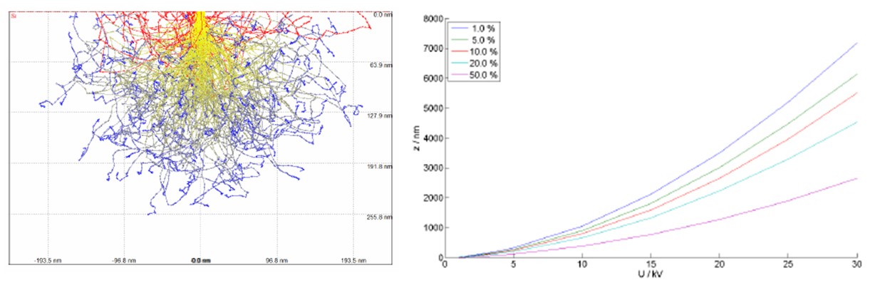
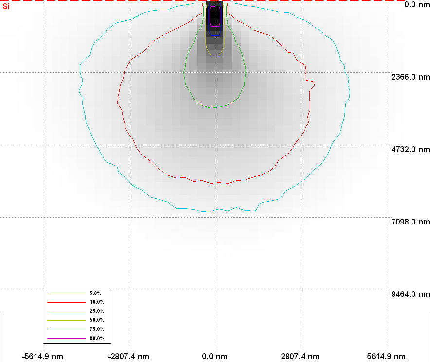
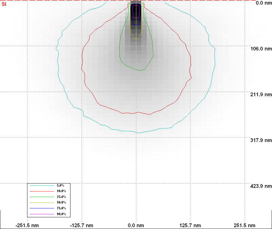
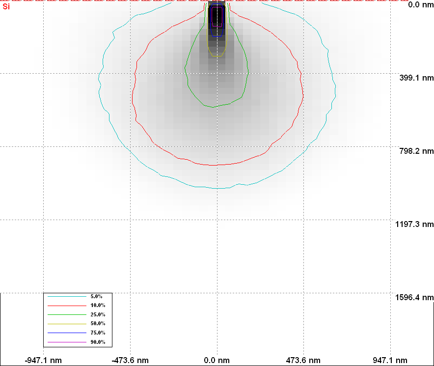
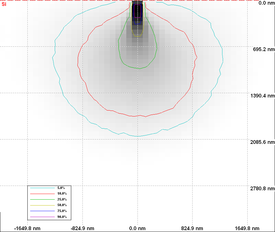
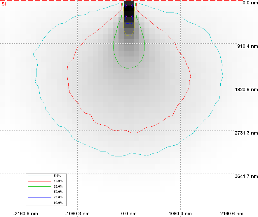
The electron beam is narrowly focused until it enters the specimen. There the electrons scatter in an interaction volume that can be microns wide. This limits the resolution of EBIC measurements. Below (left) is a simulation of trajectories that electrons take when they enter silicon. This simulation was made with the program CASINO. The plot on the right shows how the depth to which the interaction volume extends in silicon as a function of the acceleration voltage. One percent of the energy of the incoming electrons is deposited deeper than the highest dark blue line and 10% of the energy is deposited deeper than the red line. We were able to make the highest resolution images with an acceleration voltage of 5 keV.
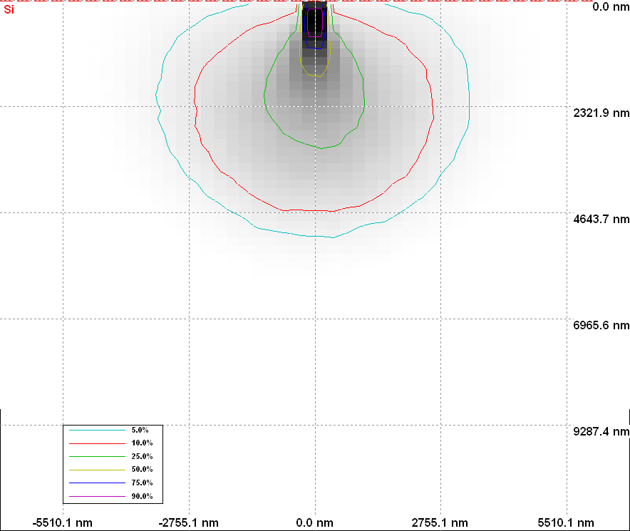
Casino can also generate plots of interaction volume for different beam energies. The image below shows the interaction volume of a 30 keV beam in silicon.
|
