1. Stacking of semiconductors
The band gap of GaAs is 1.42 eV and is direct. The band gap of AlAs is 2.16 eV and is indirect. The semiconducting alloy Al$_{x}$Ga$_{1-x}$As has a direct band gap for $x < 0.44$ and an indirect band gap for $x > 0.44$. Consider alternating layers of GaAs and Al$_{0.6}$Ga$_{0.4}$As stacked on top of each other in a periodic pattern.
- Draw the band diagram (conduction band, valence band, chemical potential) along a line perpendicular to the layers.
- Draw the carrier concentrations (electrons and holes) along a line perpendicular to the layers.
- If no voltage is applied, the total current will be zero. Nevertheless, a diffusion current can be deduced from the minority carrier concentrations. This implies that electric fields exist in this structure. Describe the diffusion currents and the electric fields.
- How could we calculate the electrical conductivity perpendicular to the layers? Keep in mind that the electrons in the conduction band are concentrated around different k values in the two materials.
Solution
Draw the band diagram (conduction band, valence band, chemical potential) along a line perpendicular to the layers.
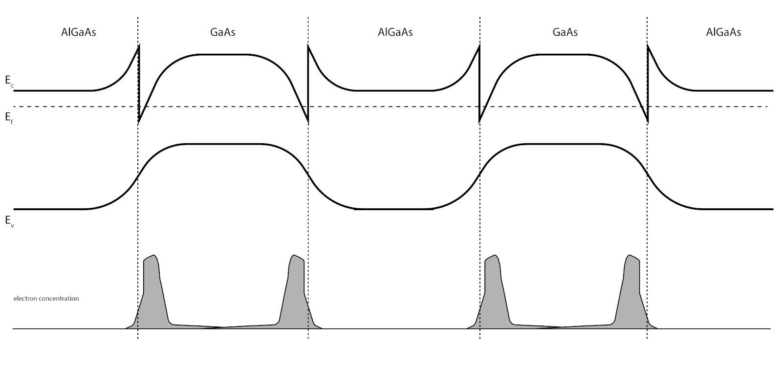 Figure 1: Bandstructure of Al$_{0.6}$Ga$_{0.4}$As / GaAs
Draw the carrier concentrations (electrons and holes) along a line perpendicular to the layers.
Answer missing.
If no voltage is applied, the total current will be zero. Nevertheless, a diffusion current can be deduced from the minority carrier concentrations. This implies that electric fields exist in this structure. Describe the diffusion currents and the electric fields.
Answer missing.
How could we calculate the electrical conductivity perpendicular to the layers? Keep in mind that the electrons in the conduction band are concentrated around different k values in the two materials.
Answer missing.
2. GaAs
GaAs is a direct band gap semiconductor with a bandgap of $E_{g} = 1.424$ eV. The electrons at the minimum of the conduction band have an effective mass of $m = 0.067m_{e}$ the light holes at the top of the valence band have an effective mass of $m_{lh} = 0.087m_{e}$, and the heavy holes at the top of the valence band have an effective mass of $m_{hh} = 0.45m_{e}$. Here is $m_{e}$ the mass of a free electron.
- Sketch the electron dispersion relation and the electron density of states near the bottom of the conduction band and the top of the valence band.
- Describe how you could use this information to calculate temperature dependence of the chemical potential of undoped GaAs.
- Describe how you can use this information to plot the optical absorption of GaAs.
Solution
Sketch the electron dispersion relation and the electron density of states near the bottom of the conduction band and the top of the valence band.
The part of the dispersion relation around the direct band gap is shown in Figure 2. Since there are light and heavy holes, two dispersion curves must meet at the top of the valence band. The effective mass determines the curvature, thus the conduction band and the light hole part of the valence band have a similar curvature, while the heavy hole curve has a much smaller curvature.
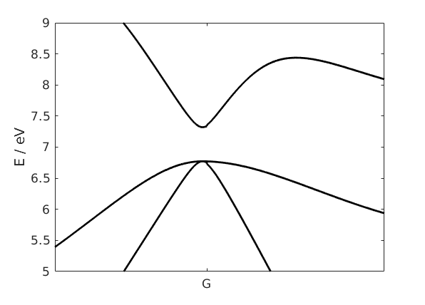 Figure 2: Band structure of GaAs at the direct band gap.
The electron density of states near the bottom of the conduction band and the top of the valence band can be calculated with the following formula:
\begin{align*} D(E) = \left\lbrace \begin{array}{ll} \frac{(2 m_h^*)^{\frac{3}{2}}}{2 \pi^2 \hbar^3} \sqrt{E_v - E}\ , & E < E_v \\ 0\,, & E_v < E < E_c\\ \frac{(2 m_e^*)^{\frac{3}{2}}}{2 \pi^2 \hbar^3} \sqrt{E - E_c}\ , & E > E_c \end{array}\right. \end{align*}The effective masses appearing in this equation are so called "density of states effective masses", which must not necessarily be equal to the effective masses from the dispersion relation, because for the density of states effective masses anisotropies and multiple bands (light and heavy holes) must be taken into account.
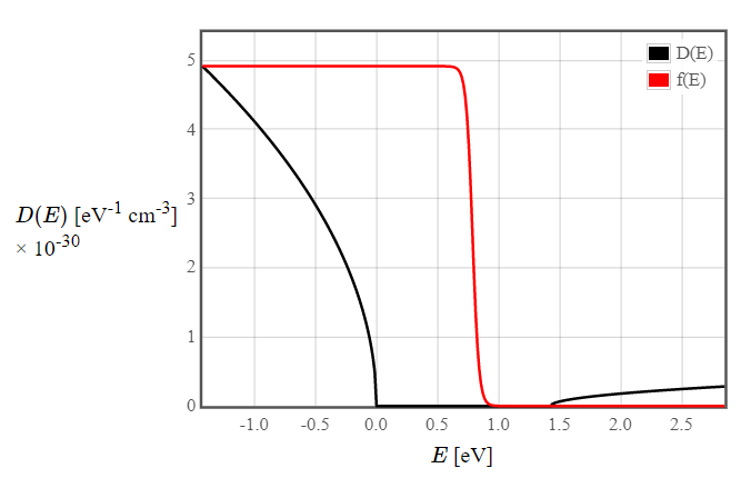 Figure 3: Density of states and Fermi function for GaAs at 300 K.
Describe how you could use this information to calculate temperature dependence of the chemical potential of undoped GaAs.
The Fermi function specifies which states are occupied. Based on this the concentration of electrons in the conduction band and the concentration of holes in the valence band can be calculated by integrating the density of states times the Fermi function in the conduction and and valence band respectively:
\begin{equation*} n = \int_{E_c}^{\infty} D(E) f(E) dE \end{equation*} \begin{equation*} p = \int_{-\infty}^{E_v} D(E) f(E) dE \end{equation*}Since the integral can not be evaluated analytically, the Fermi function is approximated using the Boltzmann approximation:
\begin{align*} f(E) &= \frac{1}{1 - \exp{\frac{E - \mu}{k_B T}}} \approx \exp{\frac{\mu - E}{k_b T}} &\text{in the conduction band,} \\ (1 - f(E)) &= 1-\frac{1}{1 - \exp{\frac{E - \mu}{k_B T}}} \approx \exp{\frac{E - \mu}{k_b T}} &\text{in the valence band.} \end{align*}The Boltzmann approximation is well justified for $\mu-E_v < 3k_BT$ and $E_c-\mu < 3k_BT$, respectively.
This yields the following concentration of electrons in the conduction band:
\begin{equation*} n = \frac{1}{\sqrt{2}} \left ( \frac{m_e^* k_b T}{\pi \hbar^2}\right )^\frac{3}{2} \exp{\frac{\mu - E_c}{k_B T}} \end{equation*}and for the holes in the valence band:
\begin{equation*} p = \frac{1}{\sqrt{2}}\left (\frac{m_h^* k_b T}{\pi \hbar^2} \right )^\frac{3}{2} \exp{\frac{E_v - \mu}{k_B T}}. \end{equation*}In an intrinsic semiconductor, the density of electrons equals the density of holes, $n = p$, and from this the chemical potential can be calculated as:
\begin{equation*} \mu = \frac{E_v + E_c}{2} - \frac{3}{4} k_B T \ln{\frac{m_e^*}{m_h^*}}. \end{equation*}Describe how you can use this information to plot the optical absorption of GaAs.
There will be no absorption up to the energy of the band gap, because there are no allowed transitions from filled states to empty states in this range. Since the density of states at the bottom of the conduction band starts off like $\sqrt{E-E_v}$ we expect a square-root like behavior of the absorption coefficient in this region:
\begin{equation*} \alpha_{abs}(\omega) \propto \sqrt{\hbar\omega-E_g}. \end{equation*}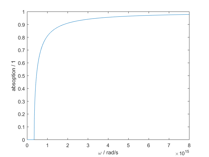 Figure 4: Plot of the optical absorption of GaAs
3. Doped Silicon
Silicon is doped with boron (an acceptor) at a concentration of 1015 cm-3.
- How could you calculate the chemical potential?
- Sketch the concentration of holes as a function of temperature.
- How could you calculate the conductivity as a function of temperature? Make a sketch of the conductivity vs. T.
- How can you experimentally determine the bandgap from the plot in (c)?
Solution
How could you calculate the chemical potential?
The chemical potential can be found by solving the charge neutrality condition numerically. One way to do this is to program the formulas for $n$, $p$, $N_D^+$, and $N_A^-$. Then choose a temperature and calculate $n$, $p$, $N_D^+$, and $N_A^-$ for every value of the chemical potential between $E_V$ and $E_C$. For one of these $\mu$ values, the charge neutrality condition will be satisfied.
When $n + N_A^-$ and $p + N_D^+$ are plotted as a function of $\mu$, the chemical potential is where the two lines cross.
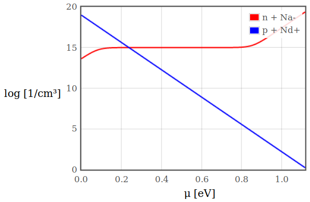 Figure 5: Plot of $n + N_A^-$ and $p + N_D^+$ with a acceptor concentration of 1015 cm-3 at a temperature of 300 K.
From this information the chemical potential can be plotted as a function of temperature:
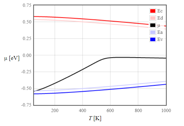 Figure 6: Temperature dependence of the chemical potential of silicon doped with boron at concentration of 1015 cm-3.
Sketch the concentration of holes as a function of temperature.
The concentration of holes can be calculated with the following formula:
\begin{equation*} p = N_V \cdot \biggl\lgroup\frac{T}{300}\biggr\rgroup^{\frac{3}{2}} ~\frac{3}{2} \exp{\frac{E_V - \mu}{k_B T}}. \end{equation*}and the concentration of electrons in the conduction band results from $np=n_i^2$. Plotted over temperature the concentrations look like this:
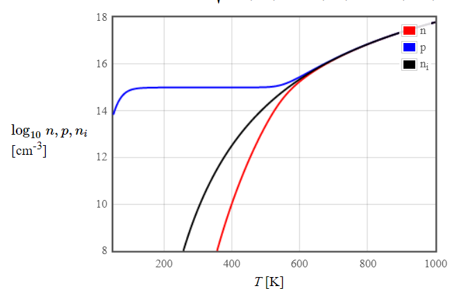 Figure 7: Concentration of holes and electrons as a function of temperature for Silicon doped with boron at a concentration of 1015 cm-3.
How could you calculate the conductivity as a function of temperature? Make a sketch of the conductivity vs. T.
The conductivity $\sigma$ of a semiconductor is defined as:
\begin{equation*} \sigma = (n\mu_e + p\mu_h)\cdot e \end{equation*}with $e$ as the elementary charge, $n$ and $p$ being the electron and hole concentration and $\mu_e$ and $\mu_p$ being the electron and hole mobility.
Because in a p-type semiconductor $N_A > N_D$ and therefore $n \approx 0$ the conductivity can be assumed to be
\begin{equation} \sigma = p \mu_h e. \label{eq:conductivity_mobility} \end{equation}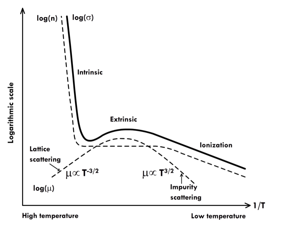 Figure 8: Conductivity, mobility and charge carrier density as functions of temperature
To calculate the mobility various scattering types have to be taken into account. In semiconductors the mobility is mainly determined by lattice scattering (i.e. scattering of charge carriers with phonons which increases with temperature) and impurity scattering (which decreases with increasing temperature).
The charge carrier density, mobility and conductivity in an extrinsic semiconductor are shown in figure 8.
How can you experimentally determine the bandgap from the plot in (c)?
At high temperatures (above ∼400 K), when the charge carrier concentration is intrinsic, the mobility is dominated by lattice scattering ($\mu \propto T^{-\frac{3}{2}}$). In this regime the conductivity varies with temperature as
\begin{equation} \sigma \approx \exp{\frac{-E_g}{2 k_b T}} \label{eq:conductivity_400K} \end{equation}By conducting a Hall measurement, the hole mobility can be determined. From the mobility one can calculate the bandgap using \eqref{eq:conductivity_mobility} and \eqref{eq:conductivity_400K}. Alternatively the conductivity can be measured directly in the intrinsic regime and the band gap calculated from \eqref{eq:conductivity_400K}.
4. Organic Semiconductor
- Describe excitons, polarons, and bipolarons in organic semiconductors. How could they be measured experimentally?
- What experiments could you do to show that the charge carriers in an organic semiconductor are holes?
- Sketch the dielectric function of an organic semiconductor.
- How would you measure the dielectric function?
- What are the limiting values for the real and imaginary parts of the dielectric function at high and low frequency?
Solution
Describe excitons, polarons, and bipolarons in organic semiconductors. How could they be measured experimentally?
See questions 6 in Electrons and 2 in Quasiparticles.
What experiments could you do to show that the charge carriers in an organic semiconductor are holes?
The type of majority charge carrier can be determined by a Hall measurement. The direction of the measurable Hall voltage $U_H$ depends on the type of charge carrier. For details on Hall effect measurements see question 2 in Electrons c.
Sketch the dielectric function of an organic semiconductor.
The dielectric function for a semiconductor is approximately given as:
\begin{equation*} \epsilon_r(\omega) = 1 + \chi_E(\omega) = 1 + \frac{n_{\omega_{0}} q^2}{\epsilon_0 m} \frac{1}{\omega_0^2 - \omega^2 + i \gamma\omega} \ . \end{equation*}Figure 9 shows an example for the dielectric function of a semiconductor.
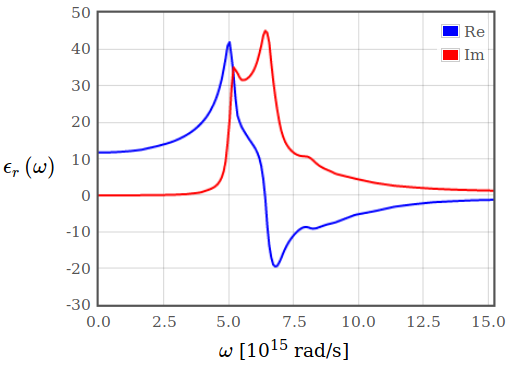 Figure 9: The dielectric function of a semiconductor.
How would you measure the dielectric function?
Since, at least for non-ferromagnetic materials with a relative permeability of nearly 1 ($\mu_r \approx 1$), the dielectric function $\epsilon_r(\omega)$ is related to both the refractive index $n$ and the extinction coefficient $K$ by the following relation
\begin{equation*} \sqrt{\epsilon_r(\omega)} = n + i K , \end{equation*}measuring both the reflectivity and the extinction coefficient is an option to indirectly measure the dielectric function.
The extinction coefficient is further related to the absorption coefficient $\alpha$ as follows:
\begin{equation*} \alpha = \frac{2 \omega K}{c} \end{equation*}so instead of measuring the extinction coefficient, measuring the absorption coefficient is one other way to measure parts of the dielectric function.
Since the real and imaginary parts of the dielectric function are related by the Kramers-Kronig relations, it is sufficient to measure one of the properties mentioned above to determine the dielectric function.
What are the limiting values for the real and imaginary parts of the dielectric function at high and low frequency?
For $\omega = 0$ the imaginary part of the dielectric function must go to zero, because it is an odd function. The real part is positive and finite for an insulator or semiconductor.
For $\omega \to \infty$ the imaginary part of the dielectric function gets zero and the real part goes to 1.