1. Metal Properties I
Many observable properties of a metal can be calculated from the $E$ vs. $k$ dispersion relation.
- How could the electron dispersion relation of a metal be measured?
- How could the electronic contribution to the specific heat be calculated from the dispersion relation?
- How could the electrical conductivity be calculated from the dispersion relation?
- How could the dielectric function be calculated from the dispersion relation?
Solution
How could the electron dispersion relation of a metal be measured?
You can measure the dispersion relation with angle resolved photoemission spectroscopy (ARPES). In this method the energy and angle of photoelectrons created by incident monochromatic ultraviolet radiation is measured. From the photoelectric effect we know that the energy of the photoelectrons will be
\begin{equation}\label{eq:photoelectric} E_{pe} = E + \hbar\omega + \Phi , \end{equation}where $E$ is the original energy of the electron in the crystal, $\hbar\omega$ the energy of the photon and $\Phi$ the work function (the energy to take out the electron from the crystal). If $\hbar\omega$ and $\Phi$ are known, then the measurement of the photoelectron energy $E_{pe}$ allows to deduce the energy that the electron had in the crystal. Since in ARPES the direction of the particle is also measured and therefore its momentum can be determined, we obtain the band structure $E(\vec{k})$.
However, since the method relies on electrons being removed from the band structure, it allows for measurements only up to the Fermi energy. For higher energies KRIPES (k-resolved inverse photoemission spectroscopy) can be used in a similar way. Here the equation \eqref{eq:photoelectric} is used the other way round by shooting electrons into the crystal and measuring the energy of photons they emit upon relaxation into lower unoccupied states.
How could the electronic contribution to the specific heat be calculated from the dispersion relation?
From the dispersion relation you could calculate the density of states $D(E)$ by counting how many states there are for every energy $E$. Since electrons are fermions, the probability that the states are occupied is given by the Fermi function $f(E)$ (in fact this is exact only for non-interacting electrons). This gives for the internal energy density
\begin{equation*} u=\int_{-\infty}^{\infty}ED(E)f(E)dE \end{equation*}and the specific heat is defined as the derivative of the internal energy with respect to temperature
\begin{equation*} c_V=\left(\frac{\partial u}{\partial T}\right)_V. \end{equation*}How could the electrical conductivity be calculated from the dispersion relation?
You can use the Boltzmann equation to calculate the distribution function $f(\vec{k})$ (see question 1 in Transport) and then the following formula for the electrical current:
\begin{equation*} \vec{j}_{elec}=-e\int\vec{v}_{\vec{k}}D(\vec{k})f(\vec{k})d^3k=-\frac{e}{4\pi^3\hbar}\int\nabla_{\vec{k}}E(\vec{k})f(\vec{k})d^3k. \end{equation*}The electric field enters through the distribution function $f(\vec{k})$ and the electrical conductivity $\sigma$ is defined by
\begin{equation*} \vec{j}_{elec} = \sigma\vec{E}. \end{equation*}How could the dielectric function be calculated from the dispersion relation?
You can calculate the optical absorption spectrum. The absorption rate is calculated using Fermi's golden rule for a transition from an occupied electron state into an empty state. Conservation of momentum requires that the two electron states have the same $\vec{k}$, because photons carry negligible momentum compared to the first Brioullin zone of the crystal electrons. The absorption coefficient $\alpha$ is related to the extinction coefficient $K$ by
\begin{equation*} \alpha=\frac{2\omega K}{c} \end{equation*}and $K$ is the imaginary part of the square root of the dielectric function. With the Kramers-Kronig relations you can calculate the real part of the square root of the dielectric function. To get the dielectric function you simply square the combined result:
\begin{equation*} \sqrt{\epsilon_r}=n+iK. \end{equation*}
2. Metal Properties II
Many observable properties of a metal can be estimated if the electron density is known.
- How is the electronic contribution to the specific heat related to the electron density?
- How is the electrical conductivity of a metal related to the electron density?
- What does a Hall effect measurement tell us about the electron density?
- To calculate the optical properties and transport properties of a free electron gas, a second parameter besides the electron density is needed. What is this second parameter and why is it needed?
- Why does the conductivity of a metal oscillate when the magnetic field is changed?
- In an EELS experiment of a metal, how would you distinguish between phonons, magnons, and plasmons?
- How could you use an EELS measurement of bulk plasmons to help sketch the dielectric function of a metal?
- Sketch the dielectric function of a metal. Indicate the relevant frequency range for microwave engineering.
Solution
How is the electronic contribution to the specific heat related to the electron density?
The specific heat $c_V$ is the derivative of the internal energy density with respect to temperature. In the Sommerfeld expansion (see http://lampz.tugraz.at/~hadley/ss1/fermigas/sommerfeldtable/sommerfeld.php) the internal energy density of a free electron gas in terms of the electron density is given by
\begin{equation*} u\approx\frac{\hbar^2}{10m^*}\left(\pi^43^5n^5\right)^{1/3}+\frac{\left(3\pi^2n\right)^{1/3}m^*}{6\hbar^2}(k_BT)^2. \end{equation*}Accordingly the specific heat of a free electron gas is
\begin{equation*} c_V \approx \frac{\left(3\pi^2n\right)^{1/3}m^*}{3\hbar^2}k_B^2T \propto n^{1/3}. \end{equation*}How is the electrical conductivity of a metal related to the electron density?
The electrical conductivity of a free electron gas is
\begin{equation*} \sigma =\frac{ne^2\tau}{m^{*}} \propto n. \end{equation*}This result can be derived either from the Boltzmann equation (http://lampz.tugraz.at/~hadley/ss2/transport/fecond.php) or from the dielectric function of a diffusive metal (http://lampz.tugraz.at/~hadley/ss2/linearresponse/dmetal.php).
What does a Hall effect measurement tell us about the electron density?
In a typical Hall effect measurement a sample is placed in a uniform magnetic field $\vec{B} = B_z\hat{z}$ and a current is driven through it in $x$-direction, i.e. $\vec{j} = j_x\hat{x}$. The current density $j_x$ is simply the current divided by the cross section area of the sample.
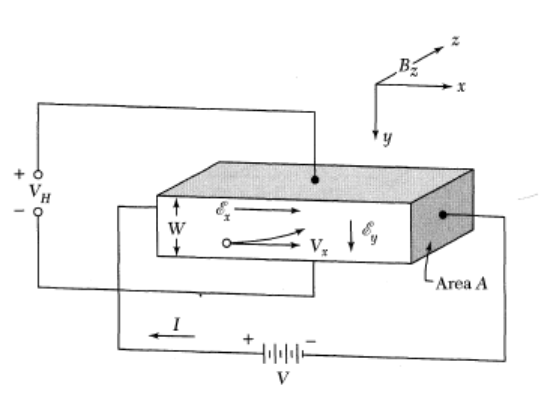 Figure 1: Setup of a Hall effect measurement.
In a diffusive regime the acceleration of the particles can be written as the drift velocity divided by the scattering time, $\vec{a} = \vec{v}_d/\tau$, leading to
\begin{equation*} m\frac{\vec{v}_d}{\tau} = -e\left(\vec{E}+\vec{v}_d\times\vec{B}\right). \end{equation*}The $y$-component of this vector equation reads
\begin{equation*} m\frac{v_{d,y}}{\tau} = -e(E_y-v_{d,x}B_z). \end{equation*}Since no current flows through an ideal voltmeter, the current and therefore the drift velocity in the $y$-direction must vanish. Writing the drift velocity in $x$-direction in terms of the current $j_x=-nev_{d,x}$ yields
\begin{equation*} E_y = -\frac{j_xB_z}{ne} =: R_Hj_xB_z \end{equation*}with the Hall constant $R_H$. The Hall constant is accessible in the experiment, because $j_x$ and $B_z$ can be adjusted and $E_y = V_H/W$, where $V_H$ is the Hall voltage measured by the voltmeter and $W$ is the width of the sample. The electron density can then be calculated from $R_H = -1/ne$.
To calculate the optical properties and transport properties of a free electron gas, a second parameter besides the electron density is needed. What is this second parameter and why is it needed?
The second parameter is the relaxation time $\tau$, see question 3 in Transport.
Why does the conductivity of a metal oscillate when the magnetic field is changed?
These are Shubnikov-de Haas oscillations (see question 4 in Magnetic Effects). However, in 3D metals they are small and can only be observed at very low temperatures.
In an EELS experiment of a metal, how would you distinguish between phonons, magnons, and plasmons?
An EELS experiment tells nothing about the type of the quasiparticles. They can only be distinguished by the energy range. Plasmons oscillate at the plasma frequency, which is typically in the ultraviolet range for metals (∼10 eV), whereas phonons have frequencies in the infrared (≲100 meV) and magnons have even lower frequencies in the microwave range (≲100 μeV).
Besides, magnons can only exist if the material is in a magnetically ordered state.
How could you use an EELS measurement of bulk plasmons to help sketch the dielectric function of a metal?
If the electrons in the EELS experiment interact with plasmons in the sample, then their energy loss will always correspond to multiples of the plasma frequency (since all plasmons have approximately the plasma frequency). Therefore the plasma frequency of the metal is simply the distance between the peaks in the EELS measurement (see figure 2).
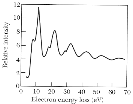 Figure 2: Example of an EELS measurement.
The plasma frequency is the frequency where the real part of the dielectric function of a metal changes from negative to positive, thus its value can help to draw the dielectric function (see next question).
Sketch the dielectric function of a metal. Indicate the relevant frequency range for microwave engineering.
The dielectric function of a diffusive metal is shown below in figure 3.
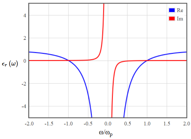
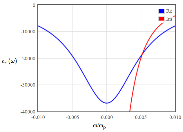 Figure 3: Dielectric function of a diffusive metal. In the left plot the function is shown for frequencies up to twice the plasma frequency $\omega_p$, in the right plot close to $\omega = 0$.
The plasma frequency is typically in the ultraviolet, thus microwave frequencies are very small compared to the plasma frequency ($\sim10^{-6}\omega_p$). Even in the right plot the relevant range would be very close to $\omega=0$.
3. Dispersion Relation
- The dispersion relation of a material is shown below. The dashed horizontal line is the energy of the highest occupied electron state. What can you deduce about this material from the band structure?
Solution
The dispersion relation of a material is shown below. The dashed horizontal line is the energy of the highest occupied electron state. What can you deduce about this material from the band structure?
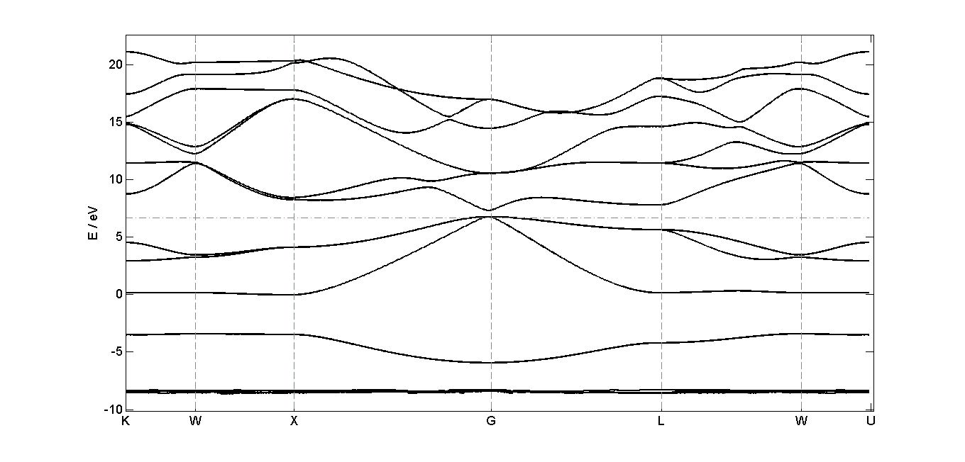
It is a direct band gap semiconductor because an electron can shift from the highest-energy state in the valence band to the lowest-energy state in the conduction band without a change in crystal momentum. We can distinguish the material from a insulator because the band gap energy is below 3 eV.
4. Fermi Surface I
- How can the Fermi surface be calculated theoretically?
- How can you measure the Fermi surface of a metal?
- Why are the states near the Fermi surface the most important for the electrical contribution to the specific heat and the thermal conductivity?
- What are electron-like orbits and hole-like orbits at the Fermi surface? How could you observe them experimentally?
- What do you expect the Fermi surface of a bcc metal with valence 1 would look like?
- How could you use a description of the Fermi surface to calculate the electronic contribution to the specific heat of magnesium?
- How could you use a description of the Fermi surface to calculate the electrical conductivity of magnesium?
Solution
How can the Fermi surface be calculated theoretically?
The first step is to calculate the energy versus $k$ relationship with some band structure method. Some methods are simple and don’t give good results like the plane wave method or tight binding, other methods are more sophisticated like the density functional theory or Hartree Fock. Once the band structure is known, the density of states can be obtained by counting how many states there are for every energy. "Filling" the density of states with electrons starting at low energy until the electron density of the material is reached gives the Fermi energy $E_f$. The Fermi surface is the surface of constant energy in $k$-space with $E=E_f$.
How can you measure the Fermi surface of a metal?
The period of the de Haas-van Alphen oscillations is indirectly proportional to the cross section of the Fermi surface with the Landau cylinders (see question 7 in Linear Response Theory). If the magnetic field is pointing in the $z$ direction the $k$ states in the $xy$ plane are restricted to circles and in the $z$ direction nothing happens. That’s why you get cylinders in 3 dimensions. If you apply a magnetic field to your metal in one direction and change the magnitude of the field, the Landau cylinders start moving through the Fermi surface, since the spacing between them is proportional to $B$. The result thereof are oscillations in all properties. Now you have to apply the magnetic field in lots of different directions to get information about the whole Fermi surface. It can happen that more than one region of the Fermi surface is parallel to the Landau cylinders. In this case you get a beating pattern, which is a modulated basic oscillation. You could Fourier transform it and that will give you the frequency components and the amplitudes of the oscillations. You can calculate the period out of the frequencies and use the following equation to match them with the corresponding cross section:
\begin{equation*} S \left ( \frac{1}{B_{n+1}} - \frac{1}{B_n} \right ) = \frac{4 \pi^2 e}{h}. \end{equation*} \begin{align*} S &\ldots ~\text{cross sectional area of the Fermi surface} \\ \left(\frac{1}{B_{n+1}}-\frac{1}{B_n}\right) &\ldots ~\text{period of the oscillations} \end{align*}Why are the states near the Fermi surface the most important for the electrical contribution to the specific heat and the thermal conductivity?
Because the low energy states are inside the Fermi sphere and cannot contribute to the specific heat or thermal conductivity, since there are no empty states they can go into. By heating up electrons are excited from states inside the Fermi surface to states outside the Fermi surface and the energy scale on which this happens is $k_BT$, which is usually much smaller than the Fermi energy. Therefore the region above and below the Fermi surface in which the states can contribute is very narrow.
Also a big Fermi surface means a bigger specific heat and thermal conductivity, because then there are more states close to the Fermi surface, which can contribute.
What are electron-like orbits and hole-like orbits at the Fermi surface? How could you observe them experimentally?
Talking about a 2D Fermi surface we look at the extended Brillouin zone scheme. There we can distinguish between parts of the Fermi surface which form closed loops enclosing occupied electron states, which are electron-like orbits, and parts of the Fermi surface which form closed loops enclosing unoccupied electron states, which are hole-like orbits. This is shown in http://lampz.tugraz.at/~hadley/ss2/fermisurface/2d_fermisurface/2dsquare.php.
The reason for these names is, that in a magnetic field electrons in electron-like orbits behave like negatively charged particles (concerning their direction of motion), whereas electrons in hole-like orbits move the other way round, like positively charged free particles.
In the case of a magnetic field $B_z$ perpendicular to the 2-D Fermi surface we have
\begin{equation*} \frac{\partial \vec{k}}{\partial t}=\vec{v}_{\vec{k}}\times \vec{B}_z \, , \end{equation*}where the group velocity is
\begin{equation*} \vec{v}_{\vec{k}}=\nabla_{\vec{k}}E(\vec{k}). \end{equation*}In hole-like orbits $\nabla_{\vec{k}}E(\vec{k})$ points inwards (because it always points outwards on the Fermi sphere and hole-like orbits have the outside of the Fermi sphere on their inside). Therefore, unlike in electron-like orbits or free electron orbits, $\vec{v}_{\vec{k}}$ is pointed in the opposite direction of $\vec{k}$ in hole-like orbits and the electrons orbit in the "wrong direction". That is, they orbit in the direction that, naively, a positively charged particle would orbit in.
This behavior can be observed e.g. in a Hall effect measurement, where the direction of the Hall voltage (or equivalently the sign of the Hall coefficient) depends on the sign of the charge (for details on Hall effect measurements see question 2 c).
What do you expect the Fermi surface of a bcc metal with valence 1 would look like?
Figure 4 shows the Fermi surface of bcc Lithium, which is a metal with valence 1. Since the volume in $k$-space of the first Brioullin zone is equal to the volume of the Fermi sphere of two electrons (due to spin) the Fermi surface is completely contained in the first Brioullin zone. Its shape is almost spherical, because it is far away from the Brioullin zone boundaries, where usually deformations occur.
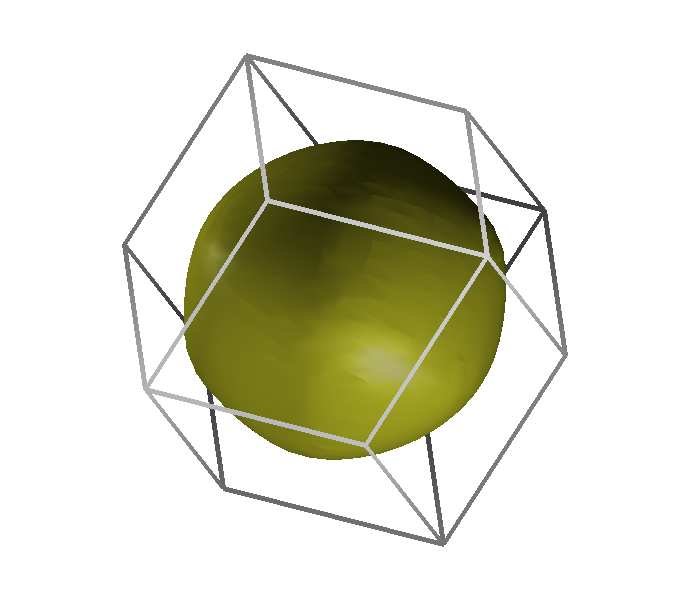 Figure 4: Fermi surface of Lithium. Taken from A. Rodriguez-Prieto & A. Bergara, Pressure Induced Fermi Surface Deformation in Lithium, 2005.
How could you use a description of the Fermi surface to calculate the electronic contribution to the specific heat of magnesium?
The specific heat is approximately given by (Sommerfeld expansion, see http://lampz.tugraz.at/~hadley/ss1/fermigas/sommerfeldtable/sommerfeld.php),
\begin{equation*} c_V = \frac{\pi^2}{3}k_B^2T D(E_F), \end{equation*}where $D(E_F)$ is the density of states at the Fermi energy. The density of states at the Fermi energy can be calculated from the Fermi surface, because the density of states in $k$-space is known and the Fermi surface contains exactly those points in $k$-space where $E=E_F$.
How could you use a description of the Fermi surface to calculate the electrical conductivity of magnesium?
Since we know the electron density $n$ of magnesium we can use the form
\begin{equation}\label{eq:el_cond_simple} \sigma=\frac{ne^2\tau}{m} \end{equation}to calculate the electrical conductivity. Here $\tau$ is the scattering time, which can be replaced by $v_F/l$, where $l$ is the mean free path of the particles and $v_F$ the Fermi velocity, which is related to the Fermi energy by $v_F = \sqrt{2E_F/m}$.
A more sophisticated calculation would use the Boltzmann equation (see question 1 in Transport) to calculate the distribution function $f(\vec{k})$. In the relaxation time approximation in an external electric field this gives (up to first order in the field)
\begin{equation*} f(\vec{k}) = f_0(\vec{k}) - \frac{e\tau}{\hbar}\frac{\partial f_0}{\partial \mu} \vec{E}\cdot\nabla_{\vec{k}}E(\vec{k}) \ . \end{equation*}In terms of the distribution function the current density is given by (see question 1 in Transport a)
\begin{align*} \vec{j}_{elec} &= -\frac{e}{4\pi^3}\int\vec{v}(\vec{k})f(\vec{k})d\vec{k} \\ &= -\frac{e}{4\pi^3}\underbrace{\int\vec{v}(\vec{k})f_0(\vec{k})d\vec{k}}_{=0} +\frac{e^2}{4\pi^3\hbar^2}\int\tau(\vec{k})\frac{\partial f_0}{\partial\mu}\nabla_{\vec{k}}E(\vec{k})(\vec{E}\cdot\nabla_{\vec{k}}E(\vec{k}))d\vec{k} \ . \end{align*}The first integral vanishes, because $f_0$ is the equilibrium distribution function and in equilibrium the current must be zero. Since the derivative of the Fermi function $\partial f_0/\partial\mu$ is sharply peaked around the Fermi energy (only the states very close to the Fermi surface contribute to the electrical conduction), it can be approximated by
\begin{align*} \frac{\partial f_0}{\partial\mu} \approx -\delta(E-E_F) \ . \end{align*}Note that this is exact at $T=0$. On the Fermi surface the volume element $d\vec{k}$ can be written as $dS\,dk_\perp$, where $dS$ is an infinitesimal element of the Fermi surface. Since the Fermi surface is a surface of constant energy, the gradient $\nabla_{\vec{k}}E$ is perpendicular to it and therefore $dE = \vert\nabla_{\vec{k}}E\vert dk_\perp$. The current now becomes
\begin{align*} \vec{j}_{elec} &= -\frac{e^2}{4\pi^3\hbar^2}\int\delta(E-E_F)\tau(\vec{k})\nabla_{\vec{k}}E(\vec{k})(\vec{E}\cdot\nabla_{\vec{k}}E(\vec{k}))dS\frac{dE}{\vert\nabla_{\vec{k}}E(\vec{k})\vert} \\ &= -\frac{e^2}{4\pi^3\hbar^2}\int\limits_{E=E_F}\frac{\tau(\vec{k})}{\vert\nabla_{\vec{k}}E(\vec{k})\vert}\nabla_{\vec{k}}E(\vec{k})(\vec{E}\cdot\nabla_{\vec{k}}E(\vec{k}))dS \ . \end{align*}Finally the electrical conductivity, which is defined by $j_{elec,i} = \sigma_{ij}E_j$, can be read off as
\begin{equation*} \sigma_{ij} = -\frac{e^2}{4\pi^3\hbar^2}\int\limits_{E=E_F}\frac{\tau(\vec{k})}{\vert\nabla_{\vec{k}}E(\vec{k})\vert}\frac{\partial E(\vec{k})}{\partial k_i}\frac{\partial E(\vec{k})}{\partial k_j}dS \ . \end{equation*}For the special case of a spherical Fermi surface the simple form \eqref{eq:el_cond_simple} is recovered.
5. Fermi Surface II
Bismuth is a semimetal with a very small Fermi surface.
- What does this tell you about the properties of Bi?
- How would you calculate the Fermi surface?
- How can you tell if the charge carriers are electrons or holes?
- How can you measure the Fermi surface experimentally?
Solution
What does this tell you about the properties of Bi?
With a very small Fermi surface, Bismuth does not have many $k$ states near the Fermi surface available and therefore will have a small specific heat, thermal conductivity and electrical conductivity.
How can you tell if the charge carriers are electrons or holes?
The Hall effect can be used to determine the signs of charge carriers in metals and semiconductors. It is well known that when electrons are charge carriers, the Hall coefficient is negative, i.e. $R_H<0$; when holes are current carriers, the Hall coefficient is positive, i.e. $R_H>0$. For details on Hall effect measurements see question 2 c.
6. Density of states at the Fermi energy I
A material is known to have zero density of states at the Fermi energy.
- What does this tell you about the electrical, thermal, and optical properties of this material?
- Which of the following quasiparticles would you expect to observe in this material? (phonons, bipolarons, excitons, polaritons, plasmons) Why?
Solution
What does this tell you about the electrical, thermal, and optical properties of this material?
If there are zero states at the Fermi energy, the material can't be a conductor because there aren't any occupied states in the conduction band at temperature $T = 0~\mathrm{K}$. It depends on the band gap whether the material is a semiconductor ($E_{gap} \lesssim 3~\mathrm{eV}$) or an insulator ($E_{gap} \gtrsim 3~\mathrm{eV}$).
If the energy of an incoming photon is higher than the band gap energy, the photon can be absorbed. Vice versa it is possible that the material emits light with energies above $E_{gap}$. In insulators photons in the optical range won’t be absorbed because the gap is too high. Furthermore most insulators are transparent because there are to too little free electrons to reflect the incoming light.
The thermal behaviour of semiconductors and insulators depends on the phonon distribution of the material. In metals conduction electrons additionally contribute to the thermal conductivity, but no electron states at the Fermi energy means no electrons to participate in thermal conduction. Usually the phonon contribution is small compared to the electron contribution and therefore insulators are poor thermal conductors compared to metals.
Which of the following quasiparticles would you expect to observe in this material? (phonons, bipolarons, excitons, polaritons, plasmons) Why?
Phonons are quantized lattice vibrations and occur in all materials.
Bipolarons are bound pairs of polarons. A polaron consists of an electron and an ionic polarization field around it. You have to distinguish between large (Fröhlich) and small polarons (Holstein). Large polarons with a high effective mass appear in ionic insulators, small polarons in organic semiconductors due the lower field. Therefore you will find bipolarons in this material since it is an insulator or a semiconductor.
Excitons are bound states of an electron and a hole in a semiconductor or an insulator. They do not appear in a metal because you can't create the electron-hole pair without the band gap. Therefore you will find excitons in our material.
Polaritons describe the coupling of a phonon with a photon. Therefore the optical phonon branch has to cross the optical dispersion. In metals the light can't propagate into the material, therefore polaritons do not occur in a metal, but they possibly do in our material since it isn't a metal. However, polaritons only exist in crystals with at least 2 atoms in the unit cell, because photons can only couple to optical phonons.
Plasmons are collective, coherent oscillations of free conduction electrons which occur when a metal is exposed to light. Therefore you won't find them in our material.
Magnons are excitations of magnetic states. It is a spin-wave, analogical to a quantized sound-wave of a phonon. Therefore you need a magnetic order like in ferro- (parallel) or in antiferromagnetic (antiparrallel) materials. Magnetic materials typically have a high density of states at the Fermi energy so we don't expect to observe magnons.
7. Density of states at the Fermi energy II
A material is known to have a high electron density of states at the Fermi energy.
- What does this tell you about the electrical properties?
- What does it tell you about the thermal conductivity and the specific heat?
- Sketch the dielectric function as a function of frequency for this material. What consequence does the high density of states at the Fermi energy have for the dielectric function?
- How could you measure the density of states at the Fermi energy?
Solution
What does this tell you about the electrical properties?
A high density of states at the Fermi energy means that this material is a good electrical conductor, because electrical conduction requires electrons to go from occupied to unoccupied states (If the Fermi sphere is filled, then all $\vec{k}$ values cancel out and there is no net current). A high density of states at the Fermi energy means that many states can contribute to electrical conductivity by making transitions from just below to just above the Fermi surface.
What does it tell you about the thermal conductivity and the specific heat?
The specific heat can be calculated via the internal energy density
\begin{equation*} u = \int_{-\infty}^{\infty} E \cdot D(E) \cdot f(E) dE = \int_{-\infty}^{\infty} \frac{E \cdot D(E)}{1 + \exp{\frac{E-\mu}{k_B \cdot T}}} dE . \end{equation*}We know that $c_V = \partial{u}/\partial{T}$, so we get the following expression:
\begin{equation*} c_V = \frac{\partial{u}}{\partial{T}} = \int_{-\infty}^{\infty} \frac{E \cdot D(E) \cdot (E-\mu) \cdot \exp{\frac{E-\mu}{k_B \cdot T}}}{k_B T^2 \left(1 + \exp{\frac{E-\mu}{k_B \cdot T}}\right)^2} dE \end{equation*}The integrand is peaked around the Fermi energy and therefore only states close to the Fermi surface contribute to the specific heat. If the density of states at the Fermi surface is large, then there are many states close to the Fermi surface which can contribute and therefore the material has a large specific heat.
Since we deal with a metal, we have a good thermal conductor because of the electron contribution to the thermal conductivity. The reason is basically the same as for the specific heat.
Sketch the dielectric function as a function of frequency for this material. What consequence does the high density of states at the Fermi energy have for the dielectric function?
Since it is a metal, the dielectric function has the typical form of a metal, as shown in figure 5. There is a large response at low frequencies, because there are many electrons close to the Fermi surface, which can react to external fields.
Figure 5: The dielectric function of a metal as a function of frequency.
$\omega_P$ ... plasma frequencyHow could you measure the density of states at the Fermi energy?
The density of states can be measured by means of Photoelectron Spectroscopy (PES), in particular UV-Photoelectron-Spectroscopy (UPS), up to the Fermi energy.
In UPS experiments the sample is exposed to monochromatic ultraviolet radiation and the energy of emitted photoelectrons is measured. The energy of the photoelectrons is (photoelectric effect)
\begin{equation*} E_{pe} = E + \hbar\omega + \Phi, \end{equation*}where $E$ is the original energy of the electron in the crystal, $\hbar\omega$ the energy of the photon and $\Phi$ the work function (the energy required to remove the electron from the crystal). If $\hbar\omega$ and $\Phi$ are known, then the energy of the electrons in the crystal can be calculated and the density of states is simply a histogram of these energies (at finite temperatures actually $D(E)f(E)$ would be obtained).
Alternatively the density of states at the Fermi surface can be measured indirectly, e.g. by measuring the specific heat
\begin{equation*} c_V \approx \frac{\pi^2}{3}k_B^2T D(E_F), \end{equation*}which is a much simpler measurement.
8. MXenes
MXenes are two-dimensional inorganic compounds consisting of thin layers of transition metal carbides, nitrides, or carbon nitrides such as Nb$_2$C and Ti$_3$CN. They are metals with a hexagonal crystal structure. There is a large electron density of states at the Fermi energy.
- What would the Fermi surface look like?
- How could you calculate the bandstructure of these materials? How could you measure the bandstructure experimentally?
- Draw the Fermi surface of graphene and compare it to the metallic MXenes.
- How can you estimate the electron density of a metal using an optical measurement?
Solution
What would the Fermi surface look like?
For a 2-D hexagonal crystal structure, the Fermi surface looks like in figure 6, depending on the number of valence electrons.
 Figure 6: Fermi surface of a 2-D hexagonal crystal
How could you calculate the bandstructure of these materials? How could you measure the bandstructure experimentally?
Use the tight binding-approach assuming two on-site energies ($\epsilon_1$ and $\epsilon_2$) for the two elements in the crystal to derive a term for the energy (like in http://lampz.tugraz.at/~hadley/ss1/bands/tightbinding/tightbinding.php for graphene). The dispersion relation in terms of the on-site energies is then given by
\begin{equation*} E = \frac{\epsilon_1 + \epsilon_2}{2} \pm \sqrt{\frac{(\epsilon_1 - \epsilon_2)^2}{2} + 4 t^2 \cdot \left (\cos{\left(\frac{\sqrt{3}}{2} k_x a\right)} \cos{\left(\frac{k_y}{2} a\right)} + \cos^2{\left(\frac{k_y}{2} a\right)} + \frac{1}{4}\right )} \ . \end{equation*}This is derived in http://lampz.tugraz.at/~hadley/ss1/bands/tbtable/dispbn.html for boron nitride, which is also hexagonal with two different atoms in the basis.
Experimental determination of the band structure is possible with ARPES, where the energy and angle of photoelectrons created by incident x-ray or ultraviolet radiation is measured.
Draw the Fermi surface of graphene and compare it to the metallic MXenes.
The dispersion relation of graphene is shown in Figure 7 with the Fermi surface indicated at $E = 0$. It consists only of the six K-points at the corners of the Brioullin zone. With the form of the dispersion relation obtained above, the material can only be metallic for $\epsilon_1=\epsilon_2$, because otherwise the two bands that arise due to the $\pm$ sign can not meet (see e.g. http://lampz.tugraz.at/~hadley/ss1/bands/tbtable/dispbn.html for the band structure of 2D boron nitride). In this case the Fermi surface consists of the same 6 points as for graphene.
However, this contradicts the statement that the density of states at the Fermi energy is large, because graphene has zero density of states exactly at the Fermi energy. Therefore the tight binding approach with one valence orbital per atom might not be suited for these materials and the real Fermi surface is bigger than only the 6 K-points (maybe rings of finite size around the K-points).
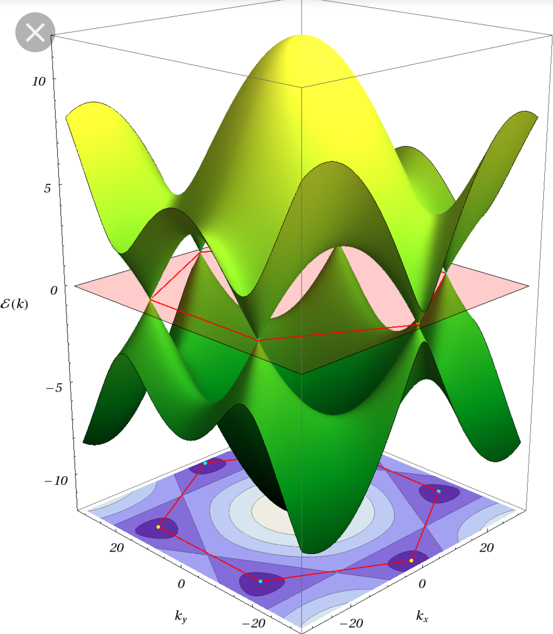 Figure 7: 3-D dispersion relation of graphene. The Fermi surface can be seen at $E = 0$ and consists only of 6 points.
How can you estimate the electron density of a metal using an optical measurement?
By means of optical measurements (PES) the Fermi energy can be determined (see question 7 c) - the Fermi energy is the highest energy appearing in the measurement at low temperatures. From the Fermi energy the electron density can be calculated using following relation:
\begin{equation*} E_F =\frac{\hbar^2}{2m} \left ( 3 \pi^2 n \right )^\frac{2}{3} \end{equation*}Another way of estimating the electron density would be measuring the plasma frequency $\omega_P$ of the metal and calculating the electron density from the definition
\begin{equation*} \omega_P = \sqrt{\frac{n e^2}{m \epsilon_0}}. \end{equation*}
9. Two-dimensional metal
- Draw the Brillouin zone of a two-dimensional metal where the charge carriers at the Fermi surface are holes.
- What experiments could you do to show that the charge carriers are holes?
- Sketch the electron density of states that corresponds to the Fermi surface you drew in (a).
- How could you measure the density of states experimentally?
- The first Brillouin zone of a two-dimensional metal is a hexagon. This metal has a valence of 2. Draw the Fermi surface in the nearly free electron approximation and indicate the regions in k-space where electrons are found and where holes are found.
- A two-dimensional metal has a rectangular Bravais lattice with primitive lattice vectors:
Solution
Draw the Brillouin zone of a two-dimensional metal where the charge carriers at the Fermi surface are holes.
In Figure 8 and Figure 9 the Fermi surface for a 2-D metal is drawn in both the extended and reduced zone scheme. Actually the Fermi surface should hit the Brioullin zone boundary at 90°, but then there would be electrons in the first or third Brioullin zone. The picture below corresponds to the empty lattice approximation.
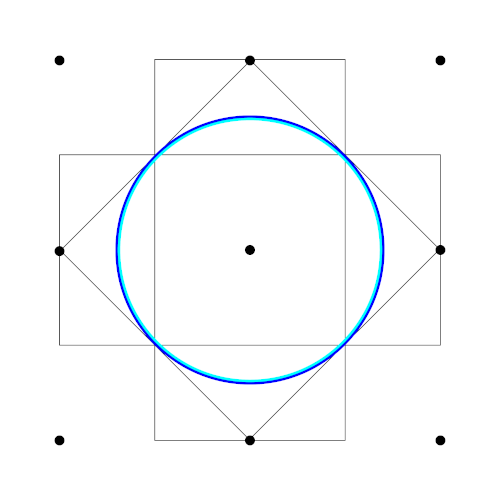 Figure 8: Fermi surface of a 2-D metal where the charge carriers are holes, drawn in the extended zone scheme
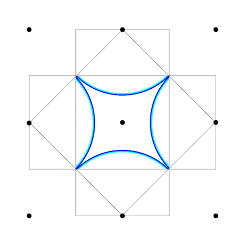 Figure 9: Fermi surface of a 2-D metal where the charge carriers are holes, drawn in the reduced zone scheme
What experiments could you do to show that the charge carriers are holes?
The direction of the Hall voltage $U_H$ in the Hall measurement depends on the type of charge carrier. This is a method to show that the charge carriers are holes. For details on Hall effect measurements see question 2 c.
Sketch the electron density of states that corresponds to the Fermi surface you drew in (a).
The first Brioullin zone is completely filled with electrons, i.e. there is one completely filled band. In the second Brioullin zone there are filled states and empty states, i.e. a half filled band. There is no gap between these bands, because both bands share a certain energy range (between the Fermi surface and the first Brioullin zone boundary).
How could you measure the density of states experimentally?
The density of states can be measured by means of Photoelectron Spectroscopy (PES), in particular UV-Photo-Spectroscopy (UPS) due to the energy range, up the the Fermi energy, or with Inverse Photoelectron Spectroscopy (IPES) above the Fermi energy.
For a description of PES see question 7 d. IPES uses the same effect the other way round by shooting electrons into the crystal and measuring the energies of emitted photons. Since they are created by electrons relaxing into lower unoccupied states, a histogram of their energies corresponds to the density of states above the Fermi surface.
The first Brillouin zone of a two-dimensional metal is a hexagon. This metal has a valence of 2. Draw the Fermi surface in the nearly free electron approximation and indicate the regions in k-space where electrons are found and where holes are found.
As the metal has a valence of 2, the area of the Fermi circle is as large as the area of the first Brillouin zone. Therefore the Fermi circle leaves the first Brillouin zone in the middle of the Brillouin zones sides. The Fermi surface meets the Brillouin zone at 90°, thus gets distorted from the circular shape. In figure 10 the Fermi surface is drawn dark on the inside. If the dark side is in the inside of a closed contour, the states on the Fermi surface are electron-like. If the light line is in the inside, the states are hole-like. In this case we have hole-like states in the first Brioullin zone at the corners and electron-like states in the second Brioullin zone at the sides.
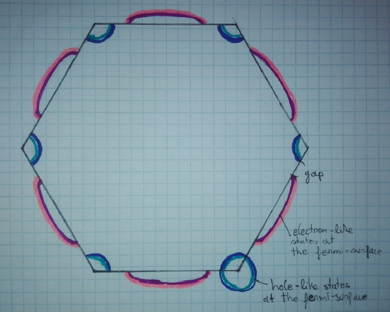 Figure 10: Fermi surface of a metal with valence 2. Taken from http://lampz.tugraz.at/~hadley/ss2/problems/exams/3oct14/index.html.
A two-dimensional metal has a rectangular Bravais lattice with primitive lattice vectors:
\begin{align*} \vec{a}_1 = a\hat{x}, \\ \vec{a}_2 = \sqrt{2}a\hat{y}. \end{align*}The metal has three valence electrons. Draw the Fermi surface indicating if the states are electron-like, hole-like, or open orbits.
In two dimensions the Fermi wave vector is given by
\begin{equation*} k_F = \sqrt{2\pi n}, \end{equation*}where $n$ is the electron density. In this case with 3 electrons per unit cell the electron density is
\begin{equation*} n = \frac{3}{a^2\sqrt{2}} \end{equation*}leading to the Fermi wave vector
\begin{equation*} k_F = \frac{\sqrt{3\pi\sqrt{2}}}{a}. \end{equation*}The dimensions of the first Brioullin zone are
\begin{equation*} \left(\frac{2\pi}{a},\frac{\sqrt{2}\pi}{a}\right) \end{equation*}and are both smaller than twice the Fermi wave vector, meaning that the Fermi surface extends into the second Brioullin zone (this is clear because the volume of the Fermi surface is equal to the volume of the first Brioullin zone already for valence 2). Since the diagonagonal of the first Brioullin zone is larger than twice the Fermi wave vector, it does not extend into the third or higher Brioullin zones.
The Fermi surface is drawn in the periodic zone scheme in Figure 11. There are hole-like states in the first Brioullin zone and electron-like states in the second Brioullin zone.
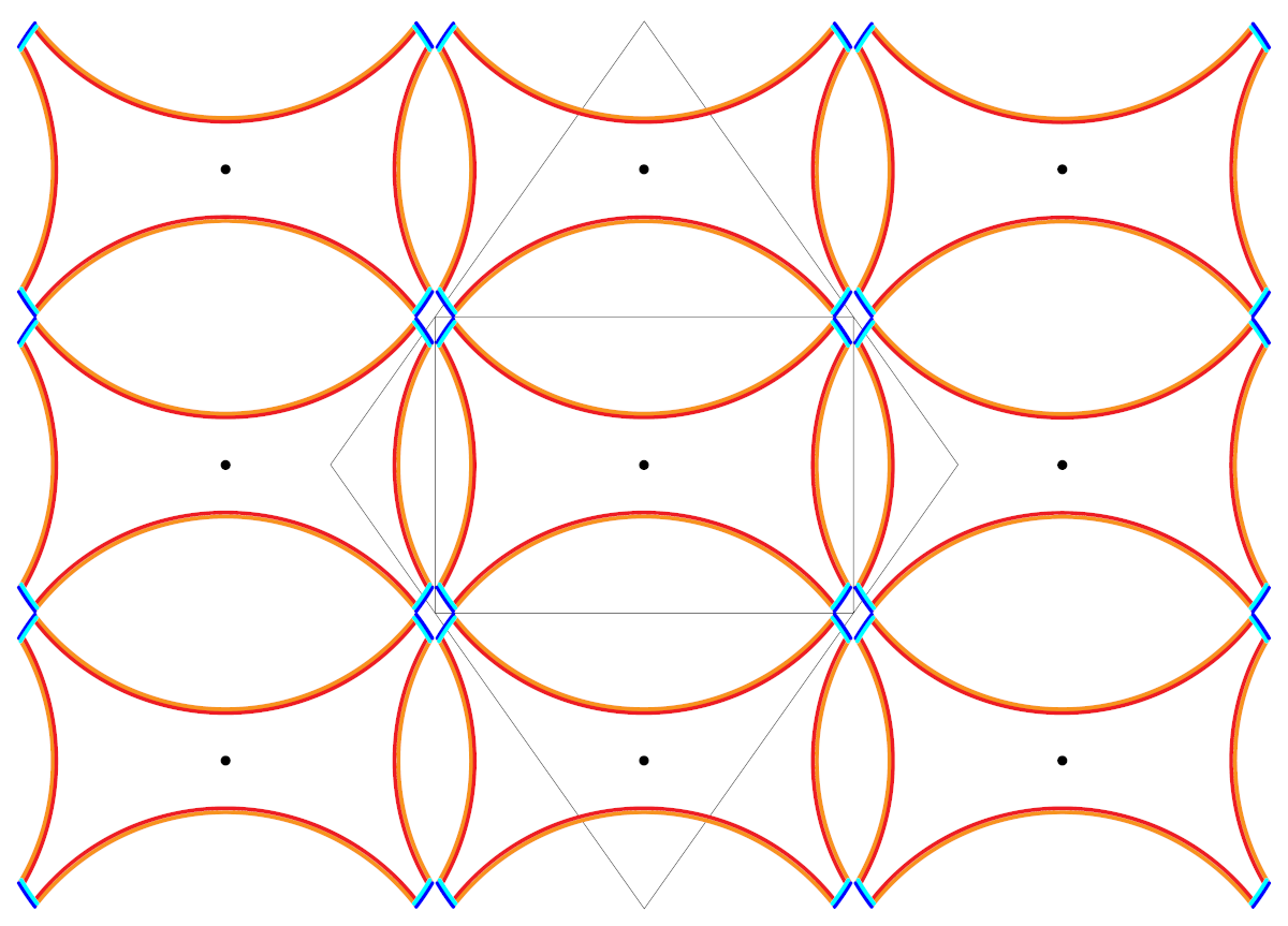 Figure 11: The Fermi surface in the periodic zone scheme, showing hole-like orbits in the first Brioullin zone (blue) and electron-like orbits in the second Brioullin zone (red).
10. Optical spectroscopy as an experimental tool for the determination of band structure
In Kittel’s book it says, "It came as a surprise that optical spectroscopy developed as an important experimental tool for the determination of band structure."
- What can optical measurements tell you about the electronic bandstructure of a material?
- How can causality be used to check optical measurements? (Causality: a bell rings after you strike it, not before you strike it.)
Solution
What can optical measurements tell you about the electronic bandstructure of a material?
By means of photo emission spectroscopy (PES) it is possible to measure the density of states up to the Fermi energy and with IPES above the Fermi energy. With angle resolved PES (ARPES) the complete band structure can be measured (see question 1 a).
Besides, optical absorption peaks occur at frequencies by which parallel bands are separated, because then many states contribute to the corresponding absorption. This is an easy experiment that can be used to check bandstructure calculations.
How can causality be used to check optical measurements? (Causality: a bell rings after you strike it, not before you strike it.)
Causality relates the real and imaginary part of response functions via the Kramers-Kronig relations. They are based on the fact, that the response must be zero for $t<0$ (i.e. before the external force starts), which requires that the even and odd part of the function are the same for $t>0$. Usually response functions are used in frequency domain, where the causality condition leads to a relation between real and imaginary part.
An example for a response function is the electric susceptibility $\chi_E$, which thus obeys the Kramers-Kronig relations. The dielectric function $\epsilon_r$ is simply $1+\chi_E$ and the square root of the dielectric function is related to the refractive index $n$ and the extinction coefficient $K$ via
\begin{equation*} \sqrt{\epsilon_r} = n+iK \end{equation*}and since the real and imaginary parts of $\epsilon_r$ are connected by the Kramers-Kronig relations, this is also the case for $n$ and $K$.
Hence, if both quantities are measured, they can be checked against each other.