1. Fermi liquid
- Explain why the Fermi function is not valid for a system of interacting Fermions.
- How does Fermi liquid theory treat electrons as nearly non-interacting Fermions?
Solution
Explain why the Fermi function is not valid for a system of interacting Fermions.
The fermi function describes an ideal fermi gas which is not the same as a fermi liquid.
For an ideal fermi gas (statistical described fermions which are not interacting with each other) the fermi function tells us the occupation probability for a given temperature that a state of energy E is occupied from a fermion.
Starting points for that are the pauli-principle and the indistinguishability of same particles.
The fermi liquid theory (or Landau theory) describes the same like a fermi gas but now with interacting fermions. Electrons from the conduction band collides with each other through their electrostatic interaction. The theory describes this kind of electron-electron interactions as quasiparticles. You can imagine quasiparticles as a field surrounding a moving electron which is caused by this electron through electrostatic effects. These quasiparticles have a one-to-one correspondence to the elementary excitations of a fermi gas. (These excitations are called quasiparticles in the fermi liquid). Then you describe the electrons as quasiparticles which have the same spin, momentum and charge, but dynamical properties like mass or magnetic moment have to get customized.
For the fermi liquid theory you start from a fermi gas in ground state (T=0K) and then raise lightly the energy which leads to low-lying excited states. For example adding a phonon to a crystal at ground state, the phonon excites the crystal (via lattice vibration) and the crystal then is in a low-lying excited state. This phonon is called a elementary excitation or quasiparticle.
Electrons, as are all half-integer spin particles, are Fermions. Thus, by the Pauli Principle, no two of them may occupy the same state. For example, if we calculate the density of electrons per unit volume
\begin{equation*} n = \int_0^{\infty} D(E) f(E,T) dE \end{equation*}where $f(E,T)$ is the probability that a state of energy $E$ is occupied, the factor $f(E, T)$ must enforce this restriction. However, for classical particles $f$ is just the statistical factor
\begin{equation*} f(E,T) = \frac{1}{1 + \exp{\frac{E-\mu}{k_B T}}} \end{equation*}which for $T=0$ would require all electrons to go into the ground state ($f(0,0) = 1$). Clearly this violates the Pauli principle.
How does Fermi liquid theory treat electrons as nearly non-interacting Fermions?
Landau argued that, if the electron-electron interaction would be turned on adiabatically, the eigenstates of the system should continuously change. The filled states then do not correspond to electrons any more, but they can be seen as fermionic excitations (quasiparticles), which still have spin $1/2$, charge $-e$ and a certain momentum $\vec{k}$ and they are still non-interacting. They have an effective mass $m^*$, which can be different from the electron mass and a different dispersion relation $E(\vec{k})$.
As long as the assumption, that the quasiparticles are non-interacting, is justified (this is the case close to the Fermi surface at low temperatures), we still have a gas of non-interacting fermions and all formulas derived for non-interacting electrons are still valid if the effective mass and the dispersion relation of the quasiparticles are used.
As interaction is turned on, the spin, charge and momentum of the fermions corresponding to the occupied states remain unchanged, while their dynamical properties, such as their mass, magnetic moment etc. are renormalized to new values.
2. Quasiparticles
- Would you expect to observe plasmons, polarons, polaritons, and excitons in a metal or an insulator?
- Could plasmons, polarons, polaritons, and excitons be observed by Raman spectroscopy? EELS? Ellipsometry?
- An Electron Energy Loss Spectroscopy (EELS) experiment is performed on a metal and there are peaks in the energy loss at 10 eV, 20 eV, 30 eV, and 40 eV. You suspect that these are due to certain quasiparticles in the metal. You perform an ellipsometry measurement to test this idea. What can the ellipsometry measurement tell you about these quasiparticles?
Solution
Would you expect to observe plasmons, polarons, polaritons, and excitons in a metal or an insulator?
Plasmons are collective, coherent oscillations of free conduction electrons which occur when a metal is exposed to light. Therefore you will find them in a metal.
A Polaron consists of an electron and an ionic polarization field around it. You have to distinguish between large (Fröhlich) and small polarons (Holstein). Large polarons with a high effective mass appear in ionic insulators, small polarons in organic semiconductors due the lower field. Therefore you will find polarons in this material since it is an insulator or a semiconductor.
Polaritons describe the coupling of a phonon with a photon. Therefore the optical phonon branch has to cross the optical dispersion. In metals the light can't propagate into the material, therefore polaritons do occur in an insulator.
Excitons are bound states of an electron and a hole in a semiconductor or an insulator. They do not appear in a metal because you can't create the electron-hole pair without the band gap. Therefore you will find excitons in an insulator.
Could plasmons, polarons, polaritons, and excitons be observed by Raman spectroscopy? EELS? Ellipsometry?
Raman spectroscopy and EELS can in principle be used to measure all quasiparticles, because they are based on inelastic scattering of light or electrons, respectively. The energy loss of these particles must be a multiple of the excited quasiparticles. However Raman spectroscopy is usually done with optical or UV frequencies, which is too low for plasmons in most materials.
Ellipsometry can give information about quasiparticles based on optical absorption. Therefore it has the same scope of application as Raman spectroscopy.
An Electron Energy Loss Spectroscopy (EELS) experiment is performed on a metal and there are peaks in the energy loss at 10 eV, 20 eV, 30 eV, and 40 eV. You suspect that these are due to certain quasiparticles in the metal. You perform an ellipsometry measurement to test this idea. What can the ellipsometry measurement tell you about these quasiparticles?
With EELS you can measure quasiparticles, because the electrons lose energy by creating these quasiparticles. It's very easy to measure plasmons (quasiparticles of the electron density waves) since electrons interact a lot with them. The measured peaks suggest a quasiparticle-energy of 10 eV (difference of two peaks; first peak: generation of one quasipartile, second peak: generation of two quasiparticles etc.), which would fit to the idea of plasmons. Ellipsometry is used to measure the polarizability of the material. The measurement can be used to calculate the dielectric function. If you know the dielectric function, you know the plasma frequency of the material (the frequency, at which the real part of the dielectric function crosses the frequency-axis). Since plasmons oscillate with the plasma frequency, you can check, if the measured frequency of the EELS measurement is the same as the plasma frequency you get with the ellipsometry measurement. If this is true, you have measured plasmons.
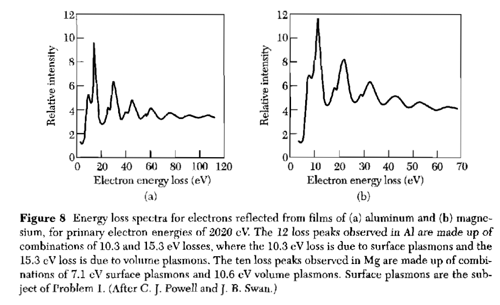 Figure 1: EELS Spectrum (taken from Kittel)
3. Plasmons
- What are plasmons?
- How would you calculate the dispersion relation ($\omega$ vs. $k$) for plasmons?
- Make a plot of the plasmon dispersion relation. Indicate roughly the values of $\omega$ (in Hz) and $k$ in (1/m) that you expect the plasmons will have.
- How could you measure plasmons?
- Do you observe plasmons in metals or insulators? Why?
Solution
What are plasmons?
We distinguish bulk (or volume) plasmons, surface (or interface) plasmons and particle plasmons. Surface plasmons are discussed in the next question.
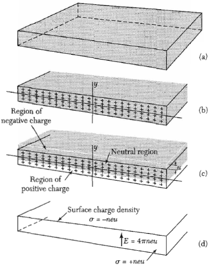 Figure 2: Illustrated plasma oscillation in a metal plate.
For the description of bulk plasmons, the first thing to know is what a plasma oscillation is. That is shown in Figure 52.1 based on a metal plate example. If we have a conduction electron gas (grey) and nearly fixed (related to the electrons) positive ion cores we have a electric neutral plasma gas. An incident electron with high energy can disturb this electrically neutral state by shifting the electron gas. This displacement u produce a surface charge density $-neu$ on the upper and $+neu$ on the lower surface ($n$...electron density). The resulting electric field tends to shift the electron gas back to the equilibrium and the gas begins to oscillate.
That means a plasma oscillation in a metal is a collective longitudinal excitation of conduction electron gas. And this oscillation is quantized, and a quantum of these plasma oscillations is called a plasmon.
We find the frequency of the longitudinal plasma oscillation where the dielectric function is zero ($\epsilon(\omega_T, K\sim0) = 0$).
How would you calculate the dispersion relation ($\boldsymbol{\omega}$ vs. $\boldsymbol{k}$) for plasmons?
The wave equation is given by
\begin{equation*} \frac{\epsilon_r}{c^2}\frac{\partial^2 \vec{E}(\vec{r}, t)}{\partial t^2} = \nabla^2 \vec{E}(\vec{r},t) \end{equation*}and the ansatz for the solution is
\begin{equation*} \vec{E}(\vec{r},t) = \vec{E}(\vec{r},\omega)\exp{i\vec{k}\cdot\vec{r}}\exp{-i\omega t}. \end{equation*}Inserting the ansatz into the wave equation yields
\begin{equation*} \omega^2\epsilon_r = c^2 k^2 \end{equation*}From the dielectric function for a collisionless metal
\begin{equation*} \epsilon_r = 1 -\frac{\omega_{P}^2}{\omega^2} \end{equation*}follows then
\begin{equation*} \omega^2 - \omega_{P}^2 = c^2 k^2 \end{equation*}and thus the dispersion relation is
\begin{equation*} \omega = \sqrt{\omega_{P}^2 + c^2 k^2}. \end{equation*}Make a plot of the plasmon dispersion relation. Indicate roughly the values of $\boldsymbol{\omega}$ (in Hz) and $\boldsymbol{k}$ in (1/m) that you expect the plasmons will have.
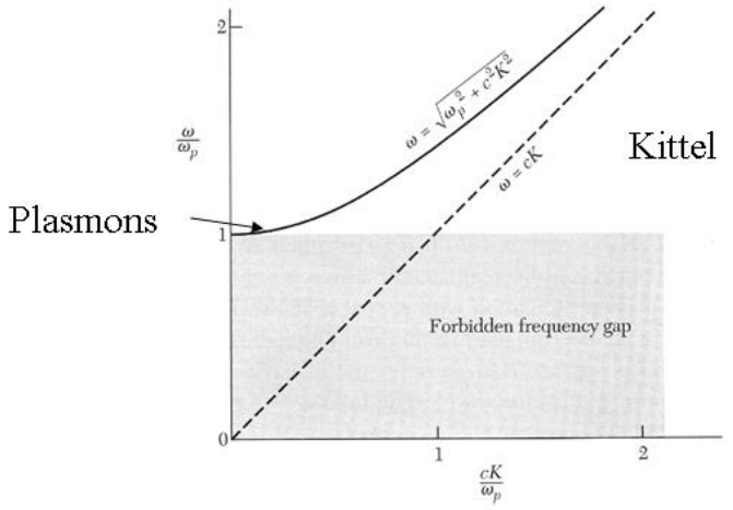 Figure 3: Dispersion relation for light in a metal. Near $k=0$ the dispersion relation bends over. At $k=0$ it has a finite value. For higher k it behaves like the normal photon dispersion relation. In the region near $k=0$ the quasiparticles are called plasmons.
The plasma frequency typically lies at $\omega \sim 10^{15}~\mathrm{Hz}$ and $k \sim 10^8 \mathrm{m}^{-1}$.
How could you measure plasmons?
The most common measurement technique for plasmons is electron energy loss spectroscopy (EELS). You accelerate electrons and shoot them through a thin specimen with a well defined energy. Then you measure the energy of the primary electrons (e.g. with an energy analyser). There you get a zero-loss peak with the energy of the incident electrons (corresponds to electrons which have not lost energy through the specimen) and you measure energies smaller than the acceleration energy, this corresponds to inelastic scattered electrons. The difference of the measured energy to the acceleration energy is the energy loss through generated plasmons for example.
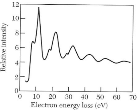 Figure 4: Energy loss spectra for electrons reflected from magnesium for primary electron energies of 2020 eV. The ten loss peaks observed are made up of combinations of 7.1 eV surface plasmons and 10.6 eV volume plasmons
Figure 4 shows a result of an EELS measurement. On the x-axis the energy loss is plotted. The y-axis shows the relative intensity. Most of the electrons will go through the sample without losing any energy. But some of them will lose $\Delta E = n\hbar\omega_P$, which is the energy you need to excite $n$ plasmons. The highest peak comes from electrons exciting one plasmon, the second from exciting two plasmons and so on.
One problem is that you can also use EELS to measure phonons, so how do you know if the measured peak comes from phonons or plasmons?
You can do an ellipsometry measurement to find the plasmon frequency and then you can check if the measured energy loss in the EELS spectrum match this frequency.
Or through through logical considerations: In this case you look at the energy of the loss and it’s at about 10-15 eV, which is above the visible (few eV) and up in the UV. The maximum frequency for phonons lies in the infrared (Debye frequency). So you know that these peaks can’t come from phonons. The peaks in Figure 4 also have a smaller peak at a lower energy and this peak comes from the surface plasmons.
Do you observe plasmons in metals or insulators? Why?
Only in metals you have the plasma from the electron gas. In dielectrics the plasma oscillation is physically the same as in the metal, but there you have no free electron gas. The reason for plasmons are that the entire valence electron gas oscillates with respect to the ion cores.
4. Surface plasmons
- What are surface plasmons and why do they only exist at an interface?
- How could surface plasmons be measured?
- Surface plasmons propagate at an interface between a metal and a dielectric. They extend a finite distance into the metal. How can this distance be calcuated from the dielectric function?
- A periodic arrays of holes are drilled into the interface. How does this modify the expression for the conservation of momentum when the surface plasmons scatter?
Solution
What are surface plasmons and why do they only exist at an interface?
Surface plasmons are coherent delocalized electron oscillations at an interface between two materials where the real part of the dielectric function changes the sign (e.g. metal and insulator).
Surface plasmons can be seen as an energy density oscillating on the surface. They have a lower energy than bulk plasmons. Which can also be seen in an EELS spectrum (4). The charge motion in the interface causes an electric field on both sides of the interface. The combination of surface plasmons and the electric fields (the total excitation) is called a surface plasmon polariton (SPP).
If there in an electric field in the metal, the charges inside the metal will try to screen the electric field which leads to a fast decay of the field in the metal. In the dielectric this happens slower.
Surface plasmons don’t have a sharp energy cause they loose energy through absorption while propagating along the interface.
They can be excited via electrons and photons. But the exciting particles have to have the same momentum and frequency (direction and wavevector) as the surface plasmon polariton needs.
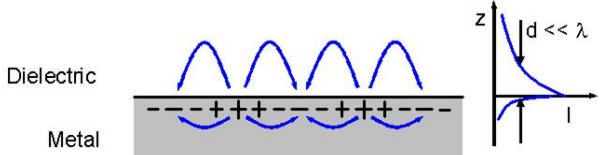 Figure 5: schematic surface plasmon (surface densitiy oscillations), right: exponential decay of electric field
Since the surface plasmons have less energy than bulk plasmons, they cannot propagate into the material and stays at the Interface. Also for existing of surface plasmons we need the two different signs from the dielectric function which is a result from solving the Maxwell equations at the boundary conditions at the interface.
(At more interest: https://www.physik.hu-berlin.de/de/nano/lehre/Gastvorlesung Wien/plasmonics; 7.2.2 bulk plasmons)
How could surface plasmons be measured?
Via EELS in the same way like described in question 4. The surface plasmons have slightly lower frequencies than bulk plasmons and therefore their excitation energies are visible in the EELS measurement as small peaks next to the larger bulk plasmon peaks.
Surface plasmons propagate at an interface between a metal and a dielectric. They extend a finite distance into the metal. How can this distance be calcuated from the dielectric function?
The propagation of electromagnetic fields in metal is limited by the skin depth. In principle it can be calculated from the following equations:
\begin{align*} \vec{j} &= \sigma\vec{E} &\text{(Ohm's law),} \\ \nabla\times\vec{B} &= \mu_0\vec{j} &\text{(Ampère's law),} \\ \nabla\times\vec{E} &= -\frac{\partial\vec{B}}{\partial t} &\text{(Faraday's law).} \end{align*}Assuming a harmonic form of the fields and a constant conductivity (which is a good approximation for low frequencies), the combined equations simplify to
\begin{equation*} k^2 = i\omega\mu_0\sigma \implies k = \frac{1}{\sqrt{2}}(1+i)\sqrt{\omega\mu_0\sigma}\ . \end{equation*}The imaginary part of the wave number describes the exponential decay in the material and the skin depth is accordingly given by its inverse,
\begin{equation*} \delta = \sqrt{\frac{2}{\omega\mu_0\sigma}}\ . \end{equation*}However, as mentioned, this is only the low frequency approximation, which is not really justified for typical surface plasmon frequencies.
A periodic arrays of holes are drilled into the interface. How does this modify the expression for the conservation of momentum when the surface plasmons scatter?
Answer missing.
5. Polarons
- What are polarons?
- What kind of materials have polarons?
- How do you measure them?
Solution
What are polarons?
A polaron is a quasiparticle used in condensed matter physics to understand the interactions between electrons and atoms in a solid material. The polaron concept was first proposed to describe an electron moving in a dielectric crystal where the atoms move from their equilibrium positions to effectively screen the charge of an electron, known as a phonon cloud. This lowers the electron mobility and increases the electron's effective mass.
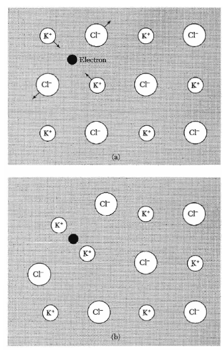 Figure 6: a) the electron and the forces on surrounding particles, b) electron plus associated strain (polaron)
A polaron is a quasiparticle consisting of an electron and an ionic polarization field in low electron density materials. Kittel states: "In an insulator the combination of the electron and its strain field is known as a polaron.".
A moving electron provides a polarization through the electrostatic forces on surrounding charges (figure 6). This cloud of polarized charges plus the electron can be described as an electron with a higher effective mass which leads to the concept of a polaron.
We differentiate between large (Fröhlich) and small polarons (Holstein). Large polarons have a very high effective mass and can be found in ionic insulators. They are much larger than the lattice constant. Large polarons typically form bands. Electrons move in bands with a large effective mass. Small polarons have a small size (in the scale of lattice constant) and occur in organic semiconductors (in soft materials the energy for making a distortion is smaller) and insulators. The electrons here are more localized and can hop through tunnelling or thermal activation.
What kind of materials have polarons?
Semiconductors and insulators. The effect is large in ionic crystals because of the strong coulomb interaction between ions and electrons. In covalent crystals the effect is weak because neutral atoms have only a weak interaction with electrons.
How do you measure them?
You can also directly see polarons with STM images, where you see the disturbed lattice and then you can say where there have to be polarons.
Another possibility are cyclotron resonance experiments, which can be used to determine the effective mass of the polarons.
6. Polaritons
- What are polaritons?
- How would you calculate the dispersion relation ($\omega$ vs. $k$) for polaritons?
- Make a plot of the polariton dispersion relation. Indicate roughly the values of $\omega$ (in Hz) and $k$ in m-1 that you expect the polaritons will have.
- How could you measure polaritons?
- Do you observe polaritons in metals, semiconductors, or insulators? Why?
Solution
What are polaritons?
Polaritons are photon – phonon collisions (means light and sound waves collisions).
More accurate: If an electromagnetic wave couples to an excited state which has a dipole moment (this could be e.g. a phonon, plasmon or an exciton) a transversal field of this coupling is generated, and a quantum of this field is called a polariton. (We discuss mainly photon-phonon interactions).
Consider the interaction of transversal optical (TO) phonons and transversal electromagnetic waves. When these two waves are in resonance (means frequency and wavevector are the same) that will change the propagation character and a forbidden band is created in the area where the two dispersion relationships of light and sound are crossing. The band is created due to avoided crossing (or also called repulsion principle). That means that in a system of two coupled oscillators with two natural frequencies, as the coupling strength increases, the lower frequency decreases and the higher increases.
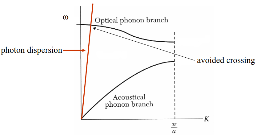 Figure 7: dispersion relation of uncoupled sound and light waves
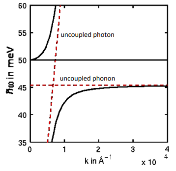 Figure 8: Phonon‐polariton dispersion relations (black lines) & dispersion relations of the uncoupled particles (red lines)
Figure 7 shows the acoustical and optical phonon branch of the phonon dispersion relation (black) as well as the photon dispersion relation (red). Since light is travelling much faster than sound the photon dispersion relation is very upright. At the point where the two lines cross, polaritons will be formed due to the avoided crossing. Because of the high slope of the photon dispersion relation, this will be at very small $k$ values.
How would you calculate the dispersion relation ($\boldsymbol{\omega}$ vs. $\boldsymbol{k}$) for polaritons?
The optical phonon modes at $k = 0$ can be modeled as a charge on a spring which satisfies the equation
\begin{equation} m\frac{d^2x}{dt^2} = -eE-Cx \label{eq1} \end{equation}where $x$ is the displacement of the charge, $E$ is the electric field and $C$ is the spring constant of the system. The atoms oscillate with the phonon frequency
\begin{equation} \omega_{T} = \sqrt{\frac{C}{m}} \label{eq2} \end{equation}Oscillation charges will also cause a polarization
\begin{equation} P = -Nex \label{eq3} \end{equation}where $N$ is the number of displaced atoms. Applying the equation \ref{eq2} and \ref{eq3} equation \ref{eq1} and assuming plane waves, we get a relationship between the electric field and the polarization for the phonons.
\begin{equation*} \frac{Ne^2}{m}E+(\omega^2-\omega_{T}^2)P = 0 \end{equation*}Now we want to obtain an analogous equation for photons in matter. We start out with
\begin{equation*} \nabla^2 E = \mu_{r} \mu_{0} \frac{\partial D}{\partial t^2} \end{equation*}and use the relation between the dielectric displacement and the electric field
\begin{equation*} D = \epsilon_{0} E + P \end{equation*}Assuming plane waves again we obtain the following formula for photons
\begin{equation*} (\mu_{0}\epsilon_{0}\omega^2 - k^2)E + \mu_{0}\omega^2 P = 0 \end{equation*}Now we received two equations that couple $E$ to $P$. There will be a solution in form of a new dispersion relation $\omega(k)$ if the following determinant is zero:
\[ \left| \begin{array}{cc} \mu_{0}\epsilon_{0}\omega^2 - k^2 & \mu_{0}\omega^2 \\ \frac{Ne^2}{m} & \omega^2-\omega_{T}^2 \end{array} \right| = 0.\]The resulting dispersion relation (figure 9) has two solutions for every $k$-value - one for the upper branch and one for the lower branch.
Make a plot of the polariton dispersion relation. Indicate roughly the values of $\boldsymbol{\omega}$ (in Hz) and $\boldsymbol{k}$ in m-1 that you expect the polaritons will have.
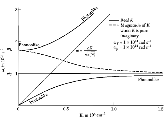 Figure 9: Phonon-polariton dispersion relation
How could you measure polaritons?
One possibility to observe polaritons is to do optical measurements, i.e. look at the reflectance of the material under investigation. (One of) the reflectance peak(s) corresponds to the band gap which arises due to the formation of polaritons.
Another way to investigate polaritons is Raman-spectroscopy. It is based on inelastic scattering of light in the sample. Through energy- and momentum conservation one receives the equations
\begin{equation*} \omega = \omega' \pm \Omega \end{equation*} \begin{equation*} \vec{k} = \vec{k}' \pm \vec{K}\pm \vec{G} \end{equation*}where ($\omega,\vec{k}$) describes the incoming photon, ($\omega',\vec{k}'$) the outgoing photon and ($\Omega,\vec{K}$) the emitted/absorbed quasiparticle. $\vec{G}$ is the reciprocal lattice vector which can always be added.
Since light carries just little momentum, only polaritons, or more general, quasiparticles with close to zero can be observed.
Looking at the energies of the outgoing photons there will be a big peak at the frequency of the incoming photons because of elastic scattering and two smaller peaks related to the generation (Stokes process) and the absorption (Antistokes process) of the quasiparticle
Do you observe polaritons in metals, semiconductors, or insulators? Why?
Polaritons as described above are typically found in ionic crystals (insulators) and can only occur in materials with 2 or more atoms per unit cell (because otherwise there are no optical phonons).
However, photons can couple to other quasiparticles than phonons in the crystal to form polaritons - for example to excitons in semiconductors or to surface plasmons in metals.
7. Excitons
By shining light on a semiconductor, excitons are created.
- Describe what an exciton is.
- By adjusting the intensity of the light, the density of excitons can be controlled. At high exciton densities, the semiconductor goes through a Mott transition. Explain what this means.
- By changing the light intensity at the frequency that creates excitons, it would be possible to adjust the plasma frequency. Explain why the plasma frequency would change. What properties of the material would be modulated by changing the plasma frequency?
Solution
Describe what an exciton is.
An exciton is a bound electron-hole pair. They are usually free to move together through the crystal. All excitons are unstable with respect to the recombination process where the electron "drops" into the hole. Excitons are formed when a photon of energy $E$ smaller than the energy gap is absorbed in a crystal:
\begin{equation*} \hbar\omega < E_g, \end{equation*}which is allowed because due to the binding energy the exciton states are slightly below the conduction band (see figure 11).
We differentiate between two extremes, the Mott-Wannier exciton and the Frenkel exciton.
Mott Wannier excitons are weakly bound and average electron-hole distance is large in comparison with lattice constant (5-10 times).
Frenkel excitons are tightly bound. In the ideal case they would travel as a wave throughout the crystal where the electron is located always close to the hole. It is essentially an excited state of a single atom, but the excitation can hop from one atom to another.
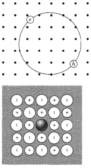 Figure 10: upper picture: Mott Wannier exciton, lower picture: Frenkel exciton
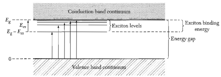 Figure 11: Energy levels of an exciton created in a direct process. Optical transitions from the top of the valence band are shown by the arrows: the longest arrow corresponds to the energy gap. The binding energy of the exciton is $E_{ex}$, referred to a free electron and free hole. The lowest frequency absorption line of the crystal at absolute zero is not $E_{ex}$, but is $E_g - E_{ex}$
By adjusting the intensity of the light, the density of excitons can be controlled. At high exciton densities, the semiconductor goes through a Mott transition. Explain what this means.
The Mott transition is a transition from insulating to metallic state of a material.
Kittel states:
A crystal composed of one hydrogen atom per primitive cell should always be a metal, according to the independent-electron model, because there will always be a half-filled energy band within which charge transport can take place. A crystal with one hydrogen molecule per primitive cell is a different matter, because the two electrons can fill a band. But let us imagine a lattice of hydrogen atoms at absolute zero: will this be a metal or an insulator? The answer depends on the lattice constant, with small values of a giving a metal and large values giving an insulator. Mott made an early estimate of the critical value a, of the lattice constant that separates the metallic state from the insulating state.
More details on Mott transitions are given in question 1 in Electron-Electron Interactions.
A similar effect can be seen in a semiconductor, where instead of decreasing the lattice constant the charge carrier density is increased. It can be understood as an overlap of the exciton wavefunctions. The bound exciton state is dissociated into unbound electrons and holes at a critical screening length $k_s$, just like the bound state of nucleus and electron in an "ordinary" Mott transition (see question 1 in Electron-Electron Interactions).
By changing the light intensity at the frequency that creates excitons, it would be possible to adjust the plasma frequency. Explain why the plasma frequency would change. What properties of the material would be modulated by changing the plasma frequency?
The plasma frequency $\omega_P$ for an ordinary metal comes easily from the definition of the dielectric constant and is defined as
\begin{equation*} \omega_P = \sqrt{\frac{4\pi n e^2}{m}}, \end{equation*}where $n$ is the electron density, $e$ is the electron charge and $m$ the electron mass. In the present case we are dealing with an electron-hole plasma and therefore the plasma frequency should depend on the exciton density. Increasing the intensity of the light leads to a higher exciton density and therefore a higher plasma frequency.
The plasma frequency determines the optical properties of a material, because below the plasma frequency light is mostly reflected out and above the plasma frequency it can propagate into the material.