Semiconductor Laboratory
|
|
Semiconductor Laboratory | |
|
|
PhotolithographyPhotolithography is a process used to make patterns on a flat substrate such as a silicon wafer or glass plate. The substrate is first coated with a thin polymer film called a resist. Light then shines through a mask so that the shadow of the mask forms a pattern on the resist. The parts of the resist that are exposed to the light are changed chemically. When the resist is subsequently placed in a developer, part of the resist is removed and the remaining resist has the same pattern as the mask. For more details, read the photolithography entry in Wikipedia, the Optical Lithography chapter in Introduction to Microfabrication by Sami Franssila, or the Photolithography chapter in MKS Handbook of Semiconductor Devices and Process Technology. There are positive resists and negative resists. Positive resists consist of long polymer chains. When these chains are exposed to light, they are cut into short pieces. The short pieces dissolve in the developer while the resist remains on the substrate in the regions which were not exposed to light. Negative resists are also long polymer chains but they crosslink under light exposure. The exposed regions of a negative resist remain after development. The resist can then be used as an etch mask. The substrate is placed in a chemical that etches the substrate but not the resist. This transfers the pattern into the substrate. After the etching, the resist is stripped off using a solvent or oxygen plasma. Alternatively, in a process called 'lift-off', a thin layer of material can be deposited over the patterned resist and then the resist can be removed by a solvent. The material that was deposited on the resist is removed but the deposited layer remains in the regions where there was no resist. The process for using Allresist AR-U 4000 as a positive resist is shown in the diagram below.
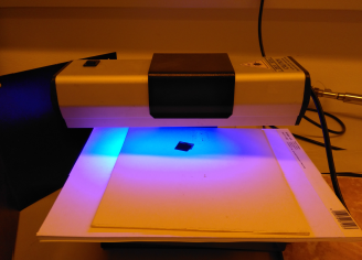
Negative resistSpin Coating For good resist wetting and adhesion, the surface shoud be hydrophobic. To check if the surface is hydrophillic or hydrophobic, a contact angle measurement can be performed. Since the contact angle of water on a clean silver surface is very small (< 10°), [1] the surface should be modified to make it hydrophobic. Soft Bake UV exposure The resist is exposed under a UV lamp for 5 minutes.
|