9.1 Bloch waves
The wave functions for electrons moving in any one-dimensional crystal can be calculated numerically. Consider the potential $\cos (\pi x)$ where $x$ is measured in Ånstroms. The period of this potential is $a=2$ Å. Use the band structure in 1-D program to determine where this potential has a band gap.
(a) Using the program to solve the Schrödinger equation for 1-D potentials, sketch the form of the wave function for an energy in a band and an energy in a band gap.
(b) What is the velocity associated with the two states you have sketched? Explain how the velocity is calculated.
9.2 Translation operator
(a) Show that $\psi(\vec{r}) = e^{i\vec{k}\cdot\vec{r}}u_\vec{k}(\vec{r})$ is an eigen function of the translation operator $\textbf{T} = l\vec{a}_1+m\vec{a}_2+n\vec{a}_3$ and determine the eigenvalue. Here $l$, $m$, and $n$ are integers and $\vec{a}_1$, $\vec{a}_2$, and $\vec{a}_3$ are the primitive lattice vectors.
(b) Consider a crystal with dimensions $N_1\vec{a}_1\times N_2\vec{a}_2\times N_3\vec{a}_3$. The number of unit cells is $N=N_1N_2N_3$. The wave functions that satisfy periodic boundary conditions have an integer number of wavelengths in the directions of $\vec{a}_1$, $\vec{a}_2$, and $\vec{a}_3$. Show that if $\vec{k}=u\vec{b}_1+v\vec{b}_2+w\vec{b}_3$ is a reciprocal lattice vector in the first Brillouin zone, a solution of Bloch form satisfies periodic boundary conditions. A useful identify is, $\vec{a}_i\cdot\vec{b}_j=2\pi\delta_{ij}$.
9.3 Kronig Penney model
An electron experiences a 1-D periodic potential, $V(x)=10 H(x-a/2)$ for $0 < x < a$. $H(x)$ is the Heaviside function. The lattice constant is $a=1.5$ Å. This potential is the of Kronig-Penney model. The band structure and the density of states can be determined analytically in the Kronig-Penney model. The lowest band is half-filled. What is the electronic contribution to the specific heat at 300 K? Use the Kronig-Penney app to determine the density of states and then use the specific heat app. Compare the result you get to the free electron model with the same electron density.
9.4 Density of states
A material is a metal if the Fermi energy lies in a band so that there are empty electron states just above the filled electron states. To determine the Fermi energy of a metal, fill the electrons into the states with the lowest energies. The energy of the highest filled state is the Fermi energy.
In a semiconductor or insulator, a band is completely filled and then there is a band gap before there are empty states in a higher band. For semiconductors the band gap is less than 3 eV and for insulators the bandgap is greater than 3 eV. At low temperatures, the Fermi energy of an insulator or semiconductor moves to the middle of the band gap.
The electron density of states for a particular material is given in the following figure. The total electron density is 20 $\times 10^{27}$ electrons/m³. The form of the density of states was chosen to make it easy to integrate (by counting squares).
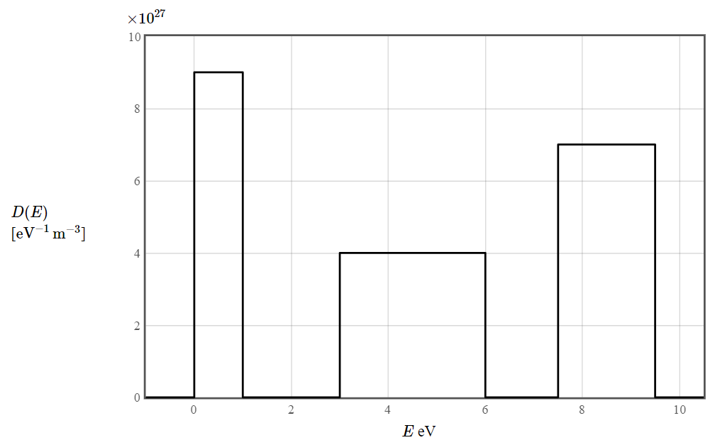
The band edges are at integer or half-integer values in eV. You can read the coordinates with the mouse: $E$ = eV, $D(E)$ = $\times 10^{27} \,[\text{eV}^{-1}\,\text{m}^{-3}]$
9.5 Aluminum
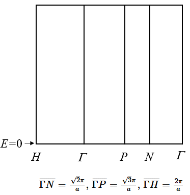
Draw the electron dispersion relation along L-Γ-X for aluminum (an fcc metal). Start with the empty lattice approximation and explain how this should be modified to include the periodic potential that the electron experiences. For fcc, $\overline{\Gamma L}= \frac{\sqrt{3}\pi}{a}$ and $\overline{\Gamma X}= \frac{2\pi}{a}$.
9.6 Bcc metal
(a) Using the empty lattice approximation, draw the electronic band structure of a bcc metal.
(b) This metal has one valence electron per unit cell. Include the Fermi energy in your drawing.
(c) $E=0$ is indicated in the plot. What is approximately the Fermi energy in electron volts if the lattice constant is $a=4.3$ Å? (You can estimate $E_F$ if you calculate the energies where the dispersion curve meets the Brillouin zone boundaries.)
9.7 Tight binding
Calculate the electron dispersion relation for a hexagonal crystal in the tight-binding approximation. Use one valence orbital per unit cell. This will result in one band. Assume there is one atom per unit cell and $c = a$.
9.8 2D Fermi surface
Consider a two-dimensional rectangular lattice with the lattice constants $a_1 = 2\pi$ Å and $a_2 = \pi$ Å with one atom in the basis. Each atom has three valence electrons. Draw the Fermi surface in the reduced and extended zone schemes.
9.9 Muffin tin potential
Consider a three-dimensional muffin tin potential U(r) consisting of spherical regions of radius $R=\frac{a}{\sqrt{3}}$ on an fcc lattice where the potential inside the spheres is $\frac{-Ze^2}{4\pi\epsilon_0r}$ and outside the spheres the potential is zero. This potential is,
$$U(\vec{r})=\frac{Ze^2}{V\epsilon_0} \sum\limits_{\vec{G}}\left(\frac{\cos(|G|R)-1}{|G|^2}+\frac{\sin(|G|R)-|G|R\cos(|G|R)}{R|G|^3}\right)\exp\left(i\vec{G}\cdot\vec{r}\right).$$Here $V=\frac{a^3}{4}$ is the volume of the primitive unit cell. An approximation for the band gap at the Brillouin zone boundary can be found by using the plane wave method and then truncating the matrix for the central equations to a $2\times 2$ matrix. Using this approximation, what is the band gap at $L$?
9.10 Electron bands
Consider a simple two-dimensional crystal with a lattice constant of $a=1$ nm and $b=3$ nm. The crystal structure forms a periodic electrostatic potential for the electrons in the form $V(\vec{r})$.
(a) Draw the electronic band structure in the empty lattice approximation along the path $X-\Gamma-Y-\Gamma-M$ where $X=\frac{\pi}{a}$, $Y=\frac{\pi}{b}$, and $M$ is the corner of the Brillouin zone.
(b) If there is one atom in the basis and each atom has three valence electrons, draw the Fermi surface in the reduced and extended zone schemes. Assume that the free electron model is applicable to draw the Fermi surface.
(c) What is the smallest value of $|k|$ on the first Brillouin zone boundary and the largest value of $|k|$ on the first Brillouin zone boundary?
(d) Draw schematically the change of the empty lattice approximation due to the periodic potential $V(\vec{r})$.
9.11 Metal, semiconductor, insulator
Classify these materials as metals, semi-metals, semiconductors, or insulators. The dotted line shows the highest occupied electron state. For semiconductors and insulators, state if the band gap is direct or indirect.
(a)  | (b) |
(c) 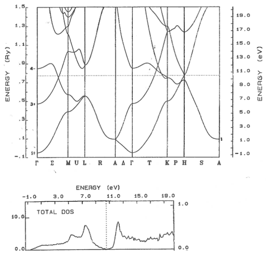 | (d)  |
(e)  | (f)  |
(g) 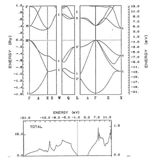 | (h)  |
9.12 Fermi function at band edges
A semiconductor has a band gap of eV. The chemical potential lies in the middle of the band gap. The probability that an electron state is occupied is given by the Fermi function $f$. What is the value of $f$ at the conduction band edge and $(1-f)$ at the valence band edge at a temperature of K?
9.13 Square wave potential
Consider an electron in a one-dimensional square wave potential with a period of 2.2 Å. The amplitude of the square wave is 3 eV.
This potential can be written as a Fourier series,
$$U(x) = \sum\limits_GU_Ge^{iGx},$$where the first few Fourier coefficients are,
$$U_0 = 0\\ U_1 = U^*_{-1}= 1.5\\ U_2 =U^*_{-2}= 0\\ U_3 = U^*_{-3}= -0.5\\ U_4 = U^*_{-4}= 0\\ U_5 = U^*_{-5}= 0.3$$If the plane wave method is used to calculate the band structure and five of the central equations are used, the corresponding matrix equation is,
$$\left[ \begin{matrix} \frac{\hbar^2(k - 4\pi/a)^2}{2m} & 1.5e & 0& -0.5e & 0 \\ 1.5e & \frac{\hbar^2(k - 2\pi/a)^2}{2m} & 1.5e & 0& -0.5e \\ 0 & 1.5e & \frac{\hbar^2k ^2}{2m} & 1.5e & 0 \\ -0.5e & 0 & 1.5e & \frac{\hbar^2(k + 2\pi/a)^2}{2m} & 1.5e \\ 0 & -0.5e & 0 & 1.5e & \frac{\hbar^2(k +4\pi/a)^2}{2m} \end{matrix} \right] \left[ \begin{matrix} C_{-2} \\ C_{-1} \\ C_0 \\ C_1 \\ C_2 \end{matrix} \right] = E \left[ \begin{matrix} C_{-2} \\ C_{-1} \\ C_0 \\ C_1 \\ C_2 \end{matrix} \right].$$What is the energy difference in eV between the lowest band and the second lowest band at $k=0$?
What is the energy difference in eV between the lowest band and the second lowest band at the Brillouin zone boundary?
Some code that might be useful for solving this problem is given in the text box below.
9.14 Magnesium
Draw the electron dispersion relation along K-Γ-M-A for magnesium (an hcp metal). Start with the empty lattice approximation and explain how this should be modified to include the periodic potential that the electron experiences. Draw the Fermi energy into your drawing. The Bravais lattice is hexagonal and there are two Mg atoms in the basis. Magnesium is in the second column of the periodic table and you can assume it has two valence electrons. For hexagonal, $\overline{\Gamma A}=\frac{\pi}{c},\quad\overline{\Gamma K}=\frac{4\pi}{3a},\quad\overline{\Gamma M}=\frac{2\pi}{\sqrt{3}a},\quad\overline{MK}=\frac{2\pi}{3a}$.
9.15 Materials Project
During the exercise, the instructor will choose a material in a certain crystalline material such as SiC-4H, ZnO (rocksalt), or FeAl3. You will be told which space group this crystal has and will be asked to find the electronic band structure of this material using the Materials Project. You will be asked if the material is a metal, an insulator, or a semiconductor.
9.16 Conduction band minimum
In silicon, the bottom of the conduction valley along the [100] direction is at $(2\pi/a)(0.85,0,0)$ where $a = 0.543$ nm. Electrons in this valley have an anisotropic effective mass. The effective mass in the [100] direction is $m_l = 0.98$ $m_e$ and the effective mass transverse to the [100] direction is $m_t = 0.19$ $m_e$. What is the energy of an electron with a $k$-vector $(2\pi/a)(0.83,0.05,0.01)$ measured from the top of the valence band?
The energy is 1.187 eV.
9.17 Germanium
(a) What is the chemical potential for intrinsic Ge measured from the top of the valence band at 300 K?
(b) Draw the density of states for Ge as a function of energy near the top of the valence band and the bottom of the conduction band.
(c) Germanium is an indirect semiconductor. The valence band maximum is at k = 0 but the conduction band minimum is in the <111> direction. How many conduction band minima are there?
(d) Describe the relationship between the effective density of states and the effective mass. (You don't need to give the formula, just describe in words how they are related.)