|
|
Physics of Semiconductor Devices |
|
|
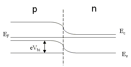
The depletion approximation for a pn junction (1)This is a relatively long problem where you will derive some important results of semiconductor physics. The answers you submit are formulas not numbers. Since these are important results, you can find the answers you need in books on semiconductor physics. Try to resist the temptation of just looking up the answers because you should understand this derivation. Consult books or other students if necessary. Consider a silicon pn junction. Far from the junction on the p-side, the Fermi energy is kBTln(Nv/Na) above the valence band edge Ev. Far from the junction on the n-side, the Fermi energy is Eg - kBTln(Nc/Nd) above the valence band edge. For zero bias voltage, the Fermi energy is the same on both sides of the junction so the valence band edge is higher on the p-side than the n-side. The difference in energy between the valence band edge on the n-side and the p-side is eVbi where Vbi is called the built-in potential.
Derive an expression for the built-in potential in terms of Na, Nd, Nc, Nv, kB, e, ni, and T. Use the expression: ni² = NcNvexp(-Eg/kBT) to eliminate Eg from the equation. The functions sin, cos, tan, asin, acos, exp, ln, and sqrt can be used. For instance, 2*sin(e*Na)*exp(kB) is a valid (but wrong) answer. Be sure to include a * to indicate multiplication; write 2*e*Na not 2eNa to multiply 2 times e times Na. It is possible that you do not need all of the variables listed above. |