Problem 1
At high electric fields, electrons gain so much energy from the applied electric field that when electrons scatter off each other, they can be scattered from the valence band into the conduction band. To be able to scatter an electron into the conduction band, the kinetic energy of the electrons must be greater than the energy gap, $E_g$. The condition, $E_g = \frac{m^*v_d^2}{2}$, can be used to estimate the critical field where impact ionization begins. Here $v_d$ is the drift velocity of the electrons.
A semiconductor has a band gap of 1 eV, an effective mass of 1 $m_e$, and a mobility of 1000 cm²/V s. Use the condition above to estimate the electric field where impact ionization will take place.
$e=1.6022\times 10^{-19}$ C $m_e=9.11\times 10^{-31}$ kg
Problem 2
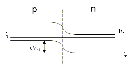
Using the formulas for the concentration of the electrons in the conducton band $n$ and the concentration of holes in the valence band $p$ derive an expression for the built-in voltage $V_{bi}$ of a $pn$-junction in terms of the doping concentrations $N_A$ and $N_D$.
Problem 3
Draw the band diagram (conduction band, valence band, Fermi energy), and the electric field as a function of position in a MOS capacitor with a p-type substrate in inversion.
Draw the electric field again for a lower concentration of acceptors in the substrate. How does the threshold voltage change when the concentration of acceptors is reduced?
Problem 4
What should be done to increase the speed of a bipolar transistor?