Ga2O3, also called Gallium(III) oxide, is a transparent ultra-wide band gap semiconductor, which garnered interest as a potential successor of gallium nitride (GaN) and silicon carbide (SiC) power semiconductor materials.
Material properties
There are five known polymorphs of Ga2O3, but interesting for semiconductor applications is beta-gallium oxide (β-Ga2O3), since it is the most stable polymorph both chemically and with regards to thermal stability.
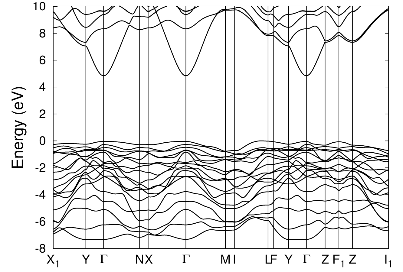
The band structure of β-Ga2O3, taken from Peelaers, Hartwin, and Chris G. Van de Walle. "Brillouin zone and band structure of β-Ga2O3." physica status solidi (b) 252.4 (2015): 828-832.
β-Ga2O3 has a monoclinic crystal structure with the space group 12 (C2/m) and an indirect band gap of 4.84 eV, while the direct band gap at Γ is only 0.04 eV larger at 4.88 eV. The maximum of the valence band is along the $I-L$ direction of the Brillouin zone, which is along one of the faces of the Brillouin zone.
Beta-gallium oxide has an expected breakdown electric field $E_b$ of 8 MV cm-1, which is more than 20 times higher than that of silicon, and 2-3 times higher than 4H-SiC and GaN. The electron mobility $\mu$ is the lowest of current power semiconductor materials, with an estimated value of 300 cm2 V-1 s-1. The relative dielectric constant ε is comparable to other materials.
Using the electron mobility μ, the breakdown field Eb and the relative dielectric constant $\epsilon_r$, one can calculate a value called Baliga's figure of merit BFOM = $\epsilon \mu E_b^3$. Baliga's figure of merit is central for power semiconductor devices and indicates the ability of the material to reproduce the details of the input signals at high voltage and low frequencies for DC currents. The BFOM for β-Ga2O3 is about 3000 times higher than that of Si, and 4-10 times higher than GaN or 4H-SiC, and is only surpassed by diamond as a semiconductor.
There are some notable material downsides of gallium oxide for device applications. The thermal conductivity of β-Ga2O3 is only 0.1 - 0.3 W cm-1 K-1, the lowest among conventional power semiconductor materials. For comparison, the thermal conductivity of bulk GaN is 8 times higher, and for bulk SiC it is 30 times higher. Hole conduction appears to be a big problem for β-Ga2O3. For p-doping, the acceptor states are deep within the band gap. Generated holes via acceptor doping are expected to trap themselves before contributing to conduction. Also, the flat structure of the valence band maximum leads to slow hole transport due to a large effective mass and thus a very low hole mobility.
Fabrication
What makes β-Ga2O3 especially enticing for large scale fabrication is that it can be grown from a melt phase with methods like the Czochralski process, floating-zone or edge-defined film-fed growth . Various epitaxy methods are currently being investigated, which include molecular beam epitaxy, metalorganic vapor phase epitaxy, halide vapor phase epitaxy and chemical vapor deposition methods.
Other materials used for power semiconductors are usually more expensive to produce. For example, 4H-SiC is grown via sublimation from the gas phase and GaN is created via epitaxy on a different bulk material, usually silicon, silicon carbide or sapphire with some additional buffer layers to counteract the lattice mismatch. One downside is the high melting temperature of beta-gallium oxide of around 1700°C. This necessitates the use of Iridium crucibles, which currently limits the potential for even cheaper wafer production.
n-doping of β-Ga2O3 was shown to be possible and relatively trivial with current doping methods like ion implantation or doping during epitaxial growth. Typically, Sn or Si is used for donor doping.
Applications
The first single-crystal β-Ga2O3 transistor was created in 2012. The device showed great characteristics for power electronics, which generated interest for more research into gallium oxide as a future wide-bandgap semiconductor. In 2013, a gallium oxide MOSFET has been successfully demonstrated in depletion mode.
Schottky Barrier Diodes are also an area of interest for β-Ga2O3, as well as MESFETs. High-electron mobility transistors (HEMT) using a two-dimensional electron gas (2DEG) are also possible with β-Ga2O3 and have been demonstrated in 2017 with modulation doped β-(Al0.2Ga0.8)2O3 / Ga2O3 heterostructures.
The high radiation hardness of the material also makes it interesting for defense and space applications. In addition to power devices, β-Ga2O3 appears to be an interesting material for deep-UV photodetectors and X-ray detectors.
Due to the lack of good hole conduction in the material, certain devices like bipolar transistors, which would rely on minority carrier conduction, are not feasible.
- Jessen, Gregg H. "The Supercharged Semiconductor: Gallium oxide could make powerful radios and switch thousands of volts." IEEE Spectrum 58.4 (2021): 36-42.
- Peelaers, Hartwin, and Chris G. Van de Walle. "Brillouin zone and band structure of β-Ga2O3." physica status solidi (b) 252.4 (2015): 828-832.
- Green, Andrew J., et al. "β-Gallium oxide power electronics." APL Materials 10.2 (2022): 029201.
- Baliga, B. Jayant. "Power semiconductor device figure of merit for high-frequency applications." IEEE Electron Device Letters 10.10 (1989): 455-457.
- Reese, Samantha B., et al. "How much will gallium oxide power electronics cost?." Joule 3.4 (2019): 903-907.
- Heinselman, Karen N., et al. "Projected Cost of Gallium Oxide Wafers from Edge-Defined Film-Fed Crystal Growth." Crystal Growth & Design 22.8 (2022): 4854-4863.
- Xue, HuiWen, et al. "An overview of the ultrawide bandgap Ga2O3 semiconductor-based Schottky barrier diode for power electronics application." Nanoscale research letters 13.1 (2018): 1-13.
- Higashiwaki, Masataka, et al. "Gallium oxide (Ga2O3) metal-semiconductor field-effect transistors on single-crystal β-Ga2O3 (010) substrates." Applied Physics Letters 100.1 (2012): 013504.
- Higashiwaki, Masataka, et al. "Depletion-mode Ga2O3 metal-oxide-semiconductor field-effect transistors on β-Ga2O3 (010) substrates and temperature dependence of their device characteristics." Applied Physics Letters 103.12 (2013): 123511.
- Wong, Man Hoi, et al. "Field-plated Ga2O3 MOSFETs with a breakdown voltage of over 750 V." IEEE Electron Device Letters 37.2 (2015): 212-215.
- Krishnamoorthy, Sriram, et al. "Modulation-doped β-(Al0. 2Ga0. 8) 2O3/Ga2O3 field-effect transistor." Applied Physics Letters 111.2 (2017): 023502.
- Hany, Ibrahim, Ge Yang, and Ching-Chang Chung. "Fast X-ray detectors based on bulk β-Ga2O3 (Fe)." Journal of Materials Science 55.22 (2020): 9461-9469.
- Chikoidze, Ekaterine, et al. "P-type β-gallium oxide: A new perspective for power and optoelectronic devices." Materials Today Physics 3 (2017): 118-126.
- Green, Andrew J., et al. "3.8-MV/cm Breakdown Strength of MOVPE-Grown Sn-Doped $\beta $-Ga 2 O 3 MOSFETs." IEEE Electron Device Letters 37.7 (2016): 902-905.
- Sasaki, Kohei, et al. "Si-ion implantation doping in β-Ga2O3 and its application to fabrication of low-resistance ohmic contacts." Applied Physics Express 6.8 (2013): 086502.