The aim of this exercise is to investigate the I-V characteristic of two LEDs (blue and white) and of a silicon signal diode. The measurements are performed with a sourcemeter unit (SMU) - Keithley 2600 Series Sourcemeter. The measurement is controlled via a Python script which is shown below.
Additionally, there is a Python script which makes one curve out of the many curves for the different current measurement ranges. It selects the part with the lowest current measurement range for each section of the curve, yielding to an accurate curve over different magnitudes of the current.
Light emitting diodes (LEDs) are a special type of diodes, which can emit light when they are used in forward bias. To get a more detailed overview over this topic, see LED-Wiki or LED - course homepage.
Due to the indirect bandgap of silicon, electrons must alter their k-vectors and transfer momentum to the crystal if they change their energetic state between valence band and conduction band. Therefore, they can't directly change the bands and emit a photon, they must do it in combination with a phonon emission to maintain momentum conservation. However, this fitting simultaneous photon and phonon emission makes this process quite improbable and so other types of semiconductors are typically used for LED's. For this reason, semiconductors like GaAs are used because they provide a direct bandgap. This direct bandgap directly corresponds to the wavelength of the emitted light.
Constructing a white LED was a long technological challenge since typical LEDs emit light of a very narrow bandwidth, while white light needs a broad spectrum. There have been established two main technologies to do that: blue LEDs which shine on a fluorescent layer (Phosphor) which emits white light after absorbing the blue light and the other technology is to mix up LEDs of red, green and blue colour to get white light. These two methods have in common that the invention of the blue LED was necessary to get them working. To get a more accurate overview over this, visit LED-Wiki.
Nevertheless signal-diodes (see: PN diode - course homepage as well as LED's both show the characteristic exponential trend of the I/V-curve described by the Shockley-equation because both kinds of diodes have the same fundamental principle of bringing a p-doped semiconductor in contact with a n-doped semiconductor.
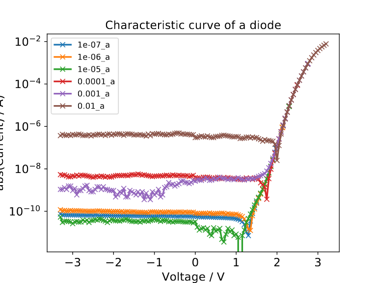
\begin{equation} I(V) = I_S(e^{\frac{eV}{nk_B T}}-1) \end{equation}$I$ describes the current through the diode, $V$ the applied voltage between anode and cathode, and $T$ the operating temperature. $k_B$ and $e$ are the Boltzmann constant and the elementary charge. The non-ideality factor is denoted by $n$ and is typically between $n=1$ and $n=2$ and hence in these the two special cases $n=1$ and $n=2$ are included in the graphs below. One main contribution to the non-ideality factor is the recombination of the charge carriers. This contribution is limited to $n=2$ because in recombination processes recombine a maximum of 2 charge carriers. The non-ideality factor can be determined with the slope of the I/V curve in a semi-logarithmic plot. The I/V curve can be retrieved by sweeping through different voltages and currents applied on the diode. To cover the diode in forward and reverse mode, the plot below shows the measured data for voltages between $-3.3 \ V$ and $+3.3 \ V$. A logarithmic scale is used because of the expected exponential behaviour and because the current is of so many different orders of magnitude.
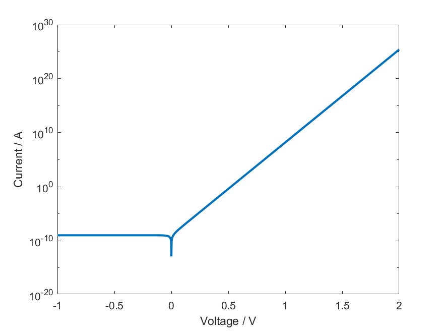
I/V-curve of the ideal diode in a semilogarithmic plot
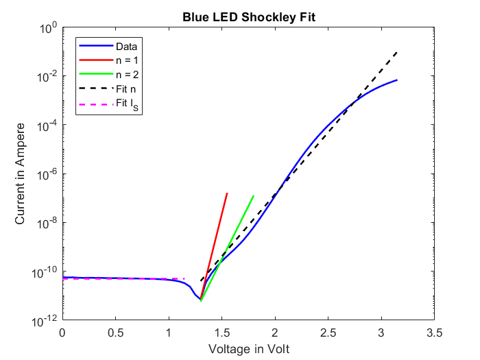
I/V-curve of the blue LED in a semilogarithmic plot. The non-ideality factor of the fitted curve is 3.43. The fitted saturation current yields $0.10 nA$.
I/V-curve of the white LED in a semilogarithmic plot. The non-ideality factor of the fitted curve is 2.39. The fitted saturation current yields $0.01 nA$.

The fitted saturation current is heavily affected by the photo current.
The plotted data shows three major differences compared to the ideal curve.
The first point is the decreased exponential growth in the upper right part of the curve. When an external voltage is applied, the energy barrier between the p-doped and n-doped area is modified. This applied voltage controls the current through the diode because if the energy barrier is lower, more electrons/holes can travel to the energetically unfavourable states on the opposite doped site due to their thermal energy. This occupation process can be approximately described via the Boltzmann distribution, yielding to the exponential growth of the current with the applied voltage as described in the Shockley equation. However, this exponential growth of the current is only possible as long as the current limitation due to the parameters except for the depletion zone is negligible. When the current is high enough the resistance of the undepleted p- and n-doped area becomes significant which leads to a flattening of the exponential growth as it can be seen in the curve.
The second point is this strange peak in the current which occurs at quite different voltages for the different ranges of the current measurement. This peak occurs when the sign of the current through the diode changes because due to the logarithmic scale it is only possible to plot the absolute value of the current, so we get a current dip when the current is near zero. When looking at the Shockley equation, we would expect the dip to be at 0 V. However, we can see in the graph that this peak occurs for voltages significantly higher than 0 V. The reason for this is that due to ambient light electron-hole pairs are produced which are separated through the electric field of the depletion zone and therefore, yield to an additional current flow in reverse direction. Therefore, we must apply a certain forward voltage to drive a current which compensates for this photo current and then we get a current of 0 A.
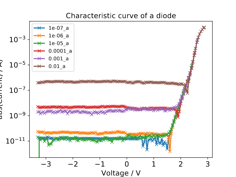
To further investigate this photo current, an additional measurement was done where the LED is placed in a dark box which should lead to a minimization of the incident ambient light. The following graph was obtained in that measurement:
One can see that the reverse current is significantly lower than in the "bright" measurement. This shows that darkening of the LED led to a significant lowering of the photo current and vice versa that the reverse current measured in the "bright" measurement was wrong due to the significant contribution of photo current with respect to the reverse current due to the applied reverse voltage. What we learnt from this measurement is that in addition to the ambient temperature, also the ambient light is a significant parameter to note when doing LED measurements.
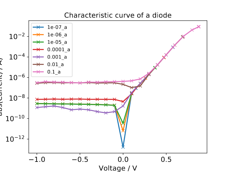
In order to make further investigation on the position of the point of zero current, there is done a measurement with a silicon signal diode where can expect that the photoeffect is negligible since it it is an indirect bandgap semiconductor and furthermore the junction is encapsulated so nearly no light can get there. In the measured plot, we can see that the point of zero current is near 0 V as expected from the Shockley equation.
In a further measurement, we want to examine if the exponential growth flattens for high currents also for this kind of diode. In order to do this, the current is allowed to go up to 0.1 A. As expected, we also get the flattening of the exponential growth for this kind of diode.
Furthermore there is a difference between the signal diode and the LED. The reverse bias current of the signal diode is about two magnitudes bigger than the reverse bias of the LED because of the wider bandgap of the LED. This leads to a lower generation of charge carriers.
If the diode is operated in reverse bias, the energy barrier between the n- and p-doped region of the valence- and conduction band for charge carriers rises and therefore, in comparison to the unbiased diode less electrons diffuse from the n-doped to the p-doped region. For holes the same applies but in the opposite direction. Charge carriers can still be generated because of thermal energy. If the energy of the bound electrons exceed the binding energy on the n-doped region, they get accelerated by the electric field of the positive potential. The holes move towards the negative potential in the p-doped region. This phenomena leads to the reverse bias current that is mainly dependending on the temperature and the bandgap. This reverse bias current of an ideal diode is the saturation current in the Shockley-equation. Therefore it can also be fitted from the I/V curve in forward bias. The exponent of the saturation current is the constant of a linear fit in the semilogarithmic plot of the I/V curve. The saturation current can be obtained by calculating the exponential of this fitting parameter. However, this is only valid for ideal diodes. For real diodes one must fit a constant of the curve in the semilogarithmic plot before the dip where the current turns positive. The saturation current depends on the temperature in the following way
\begin{equation} I_{S}(T) = c \cdot T^3 \cdot e^{\frac{E_G}{k_B T}} \end{equation}$E_G$ denotes the bandgap of the diode. If the diode is operated at room temperature the cubic term of the reverse bias current is negligible in comparison to the exponential term.
\begin{equation} I_{S}(T) = c \cdot e^{\frac{E_G}{k_B T}} \end{equation}Compared to signal diodes LEDs are not as good shielded against light. That is the reason why the LED should be exposed to the slowest possible light intensity. The bandgap can be determined with the slope of the I/T-curve in an arrhenius plot.
\begin{equation} E_G = k \cdot k_B \end{equation}$k$ is the slope of the I/T curve in the arrhenius plot.
In LED`s light is emitted if electrons change from the conduction band to the valence band. The energy difference is emitted as light with the wavelength $\lambda$.
\begin{equation} \lambda = \frac{c \cdot h}{E_G} \end{equation}c is the speed of light and h the Planck's constant. From this formula follows that one could measure the bandgap directly from the spectrum of the LED (apparently this does not work for the white LED) when it is forward biased.
As LED`s emit light when a current is driven through them in forward bias the reversed effect the photoeffect can also be observed. If light with a short enough wavelength or respectively a high enough energy is used a voltage and current can be measured. If a light source with variable wavelength is used the bandgap can be calculated.
In this chapter, we discussed various methods to extract the bandgap of a diode/LED. However, there was not done an evaluation of the bandgaps because this would require spectrographic measurements or measurements in the thermal chamber, which could both not be performed by us for time reasons.
However, there is a relation between the threshold voltage and the bandgap of a material. Some resources claim that the bandgap is equal to the threshold voltage but this is not true, which can be easily seen by the example silicon where the threshold voltage is typically around 0.7 V while the bandgap is around 1.1 eV. The built-in voltage $V_0$ and the bandgap $E_g$ are related by the following formula:
\begin{equation} eV_0 = E_g-k_B T\ln(\frac{N_V N_C}{N_A N_D}) \end{equation}With $N_V$ and $N_C$ the effective density of states of the valence band respectively conduction band. $N_A$ denotes the acceptor concentration and $N_D$ denotes the donor concentration. $T$ denotes the temperature and $V_0$ denotes the built-in voltage and we can see that there is a relation between those two but they are not directly equal. So we could estimate the bandgaps by the threshold voltages obtained from the I/V curves. However, as discussed before for the silicon, this is such a rough estimation that it makes no sense to list those values here.
In order to make further investigation on the position of the point of zero current, there is done a measurement with a silicon signal diode where it can be expected that the photoeffect is negligible since it is an indirect bandgap semiconductor and furthermore the junction is encapsulated so nearly no light can get there. In the measured plot, we can see that the point of zero current is near 0 V as expected from the Shockley equation.
In a further measurement, we want to examine if the exponential growth flattens for high currents also for this kind of diode. In order to do this, the current is allowed to go up to 0.1 A. As expected, we also get the flattening of the exponential growth for this kind of diode.

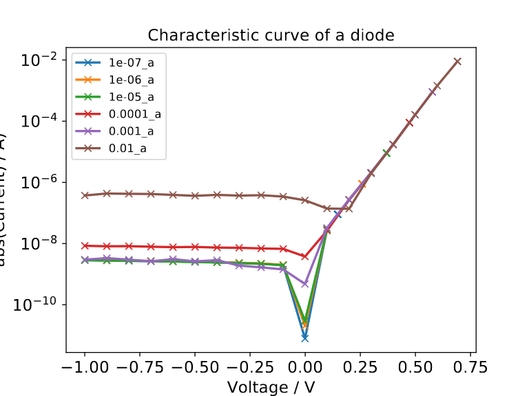
Additionally, there was performed a fit of the current to the Shockley equation, which gave the following result:

I/V-curve of the signal-diode in a semilogarithmic plot. The non-ideality factor of the fitted curve is 2.96.
In our measurements the non-ideality factor is greater than 2. This is a combination of recombination of the charge carriers and other non-idealities of the diode. Problematically, the step width was only chosen with 0.1 V because we wanted to perform a fast measurement and hence maybe some curve details got lost because of this too large spacing.
One can see that the slope of the I/V curve drops especially in the area where the voltage is between 0.8 V and 0.9 V. This is due to the fact that this an area where the series resistance of the doped substrate becomes relevant as current limitation. One can model the diode by an ideal diode with a series resistor:
When the voltage gets high, the voltage drop across the diode becomes nearly constant and more and more voltage drops across the series resistor $R_S$. So by calculating the slope of the curve for the region with the highest forward current/voltage, one can get the resistance by taking the reciprocal value of this slope.
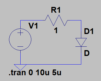
\begin{equation} R_S = \frac{\Delta V}{\Delta I}=\frac{1}{\frac{\Delta I}{\Delta V}} \end{equation}To check the region where this model gives reasonable results, there were carried out some simulations with an ideal diode with a series resistance of 1 $\Omega$. There are shown two different simulation graphs below. In the ideal case, one should get a slope of 1 A/V. However, one can see that 1 A/V is only approached asymptotically for high voltage/current. Therefore, the fit with the measured data in the region between 0.8 V and 0.9 V should give a systematic overestimation of the series resistance.
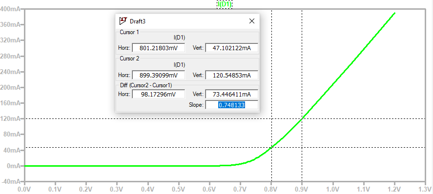
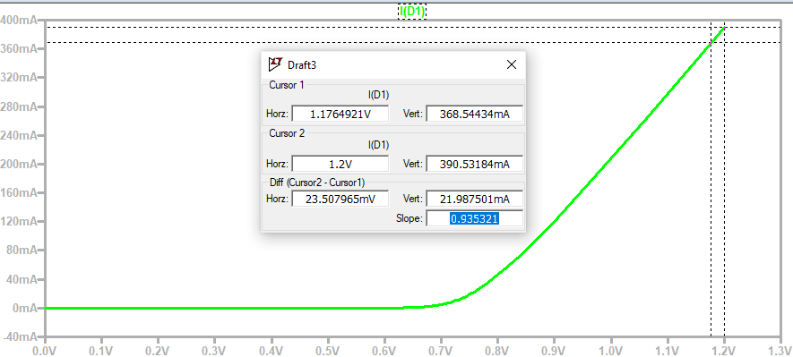
One can see from that simulations that one would really have to drive the diode near its current limitations to get accurate values for the series resistance. For our measurement, this was not the case but at least it should be a good approximation for the real value as can be seen from the simulations above. The series resistance was calculated with a value of 1.6 $\Omega$. As explained above this value should be a bit overestimated and it is suggested for further groups to go to higher currents near the current limit of the device and to use finer voltage spacing to be able to extract a more accurate value of the series resistance