Quantum phenomena in nanoscale
structures -
P. Hadley
One fascinating and potentially useful aspect of nanotechnology is
that nanostructures can be made that behave quantum mechanically. Quantum
mechanics are the laws of physics that are normally associated with the
motion of subatomic particles such as electrons, protons, and neutrons.
This description tells us that the electrons swarm around the nucleus of
the atom in an electron cloud that has a diameter of a few tenths of a
nanometer. It is hard to measure the quantum mechanical behavoir of single
atoms directly because the measurement tools we presently have are typically
much larger than an atom. One way around this problem is too find a way
to increase the size of the atom. Artificial atoms can be constructed with
sizes much bigger than ordinary atoms. For instance, embedding the atom
in a semiconductor crystal can increase the diameter of the electron cloud
of an atom. Figure 1 shows and image of the electron cloud of a silicon
atom that has been embedded in a semiconducting crystal of GaAs. The stripes
in the figure are rows of the atoms of the semiconductor and the large
bump is the electron cloud of the silicon atom. The diameter of the electron
cloud of the silicon atom has been increased to a few nanometers. At this
length scale it is possible to put an electrical contact close to the silicon
atom and by applying a voltage to that electrode it is possible to deform
the electron cloud of the individual silicon atom. This sort of interaction
between the macroscopic world of electrical contacts and microscopic world
of atoms is an important aspect of science at a nanometer scale.
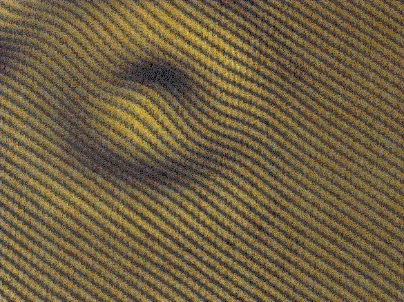 Figure 1. The large structure is
the electron cloud of a single silicon atom and the fine structure is the
atomic lattice of the GaAs crystal. (M.C.M van der
Wielen, A.J.A van Roij, and H. van Kempen, University of Nijmegen)
One of the possible applications of such artificial atoms is a quantum
computer. Quantum computing makes use of coherent states to process information.
Rather than the sequential discrete logic of conventional information processing,
use is made of quantum superposition of so called qubits. Quantum computers,
if they would exist, could perform complicated tasks faster
than conventional computers. For the realization of quantum computers the
emphasis has so far been on quantum optics, using trapped atoms or ions.
Nanotechnology could make solid state quantum devices for quantum computing
possible.
Figure 1. The large structure is
the electron cloud of a single silicon atom and the fine structure is the
atomic lattice of the GaAs crystal. (M.C.M van der
Wielen, A.J.A van Roij, and H. van Kempen, University of Nijmegen)
One of the possible applications of such artificial atoms is a quantum
computer. Quantum computing makes use of coherent states to process information.
Rather than the sequential discrete logic of conventional information processing,
use is made of quantum superposition of so called qubits. Quantum computers,
if they would exist, could perform complicated tasks faster
than conventional computers. For the realization of quantum computers the
emphasis has so far been on quantum optics, using trapped atoms or ions.
Nanotechnology could make solid state quantum devices for quantum computing
possible.
One of the difficulties in coupling the macroscopic world to the microscopic
world is bringing probes close enough to a nanostructure to be able to
measure it. Figures 2 and 3 show how a small metallic cluster and a carbon
nanotube have been coupled to electrical leads so that they can be measured.
The nanotube is only a few atoms thick. A close-up image of a carbon nanotube
is shown in Fig. 4. It is possible to manipulate the nanotubes on the substrate
by pushing them with an atomic force microscope (AFM) tip and it is possible
to cut the nanotubes into segments by applying a voltage pulse to an STM
tip.
 Figure 2. A 20 nm Pd particle (yellow)
that has been electrostatically trapped between two electrodes (red).
(A. Bezryadin, Delft University of Technology)
Figure 2. A 20 nm Pd particle (yellow)
that has been electrostatically trapped between two electrodes (red).
(A. Bezryadin, Delft University of Technology)
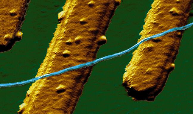
Figure 3. A single carbon nanotube
connected to two electrical leads. (Sander Tans, Delft University of Technology).
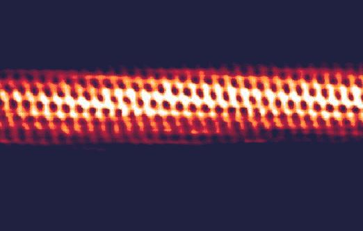
Figure 4. Atomic resolution image of a carbon nanotube. The diameter of the tube and the twist of the atomic arrangement along the tube determines the electrical conductivity of the tube. (Jeroen Wildoër, Delft University of Technology).
Using nanofabrication it is possible to create a large variety of structures
that exhibit quantum effects. Figure 4 shows a copper surface has been
modified by the addition of some iron atoms. The images show how the electron
clouds of the copper surface electrons have been modified by the addition
of the iron atoms. The interference patterns visible are a manifestation
of the wave nature of electrons.
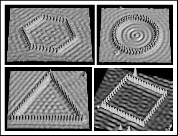 Figure 4. Iron atoms placed on copper
surface. Courtesy of Don
Eigler, IBM.
Figure 5 shows a vertical quantum dot that was fabricated at NTT in Japan.
The electrons in this structure are trapped in a thin disc between two
tunnel barriers. Measurements show that the electrons behave as if they
were part of a two dimensional atom.
Figure 4. Iron atoms placed on copper
surface. Courtesy of Don
Eigler, IBM.
Figure 5 shows a vertical quantum dot that was fabricated at NTT in Japan.
The electrons in this structure are trapped in a thin disc between two
tunnel barriers. Measurements show that the electrons behave as if they
were part of a two dimensional atom.
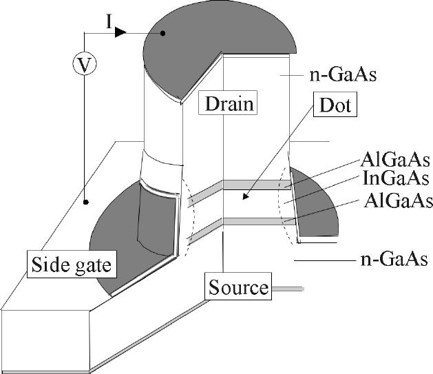 Figure 3. Schematic drawing of a
vertical quantum dot. A two dimensional disc-like atom is formed in a semiconducting
structure at the position labeled "Dot" in the figure. (S. Tarucha, NTT,
Japan)
Figure 6 shows the data that is used to determine the amount of energy
that is necessary to add an additional electron to the vertical quantum
dot of Fig. 5. This energy is the ionization energy of a disc-like atom.
Two-dimensional atoms have a different shell structure than three-dimensional
atoms. Whole new periodic tables need to be drawn up to describe these
atoms. These artificial atoms have properties that can be very different
than the properties of real atoms. For instance, it is possible to couple
a thousand times more magnetic flux to an artificial atoms than to real
atoms simply because the artificial atoms are bigger. This enables the
study of magnetically induced atomic states are inaccessible in the realm
of real atoms. We are just beginning to be able to couple these artificial
atoms together to make artificial molecules and artificial materials. These
artificial atoms can be manipulated by electric and magnetic fields in
ways not possible with real atoms. Having new atoms with properties that
can be tuned could have many applications.
Figure 3. Schematic drawing of a
vertical quantum dot. A two dimensional disc-like atom is formed in a semiconducting
structure at the position labeled "Dot" in the figure. (S. Tarucha, NTT,
Japan)
Figure 6 shows the data that is used to determine the amount of energy
that is necessary to add an additional electron to the vertical quantum
dot of Fig. 5. This energy is the ionization energy of a disc-like atom.
Two-dimensional atoms have a different shell structure than three-dimensional
atoms. Whole new periodic tables need to be drawn up to describe these
atoms. These artificial atoms have properties that can be very different
than the properties of real atoms. For instance, it is possible to couple
a thousand times more magnetic flux to an artificial atoms than to real
atoms simply because the artificial atoms are bigger. This enables the
study of magnetically induced atomic states are inaccessible in the realm
of real atoms. We are just beginning to be able to couple these artificial
atoms together to make artificial molecules and artificial materials. These
artificial atoms can be manipulated by electric and magnetic fields in
ways not possible with real atoms. Having new atoms with properties that
can be tuned could have many applications.
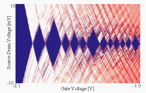 Figure 6. The current through a vertical
quantum dot as a function of the gate voltage and the bias voltage. The
size of the blue diamonds determines the ionization energy of this artificial
atom. (L.P. Kouwenhoven, Delft University of Technology)
Another example of a quantum effect in a nanostructure is the single-electron
charging effect. This arises due to the finite energy needed to charge very small structures with a single electron.
This effect can be used to monitor and manipulate individual electrons.
Charging effects can be used to construct a three terminal device called a single-electron tunneling (SET) transistor. Logic and memory circuits can be made using
SET transistors. Unlike conventional semiconductor transistors,
single-electron tunneling transistors can be scaled down to atomic dimensions.
The current that flows through a superconducting single-electron tunneling
transistor is shown in Fig. 7. The pattern repeats itself horizontally
each time another electron tunnels onto the central island of a single-electron
tunneling transistor.
Figure 6. The current through a vertical
quantum dot as a function of the gate voltage and the bias voltage. The
size of the blue diamonds determines the ionization energy of this artificial
atom. (L.P. Kouwenhoven, Delft University of Technology)
Another example of a quantum effect in a nanostructure is the single-electron
charging effect. This arises due to the finite energy needed to charge very small structures with a single electron.
This effect can be used to monitor and manipulate individual electrons.
Charging effects can be used to construct a three terminal device called a single-electron tunneling (SET) transistor. Logic and memory circuits can be made using
SET transistors. Unlike conventional semiconductor transistors,
single-electron tunneling transistors can be scaled down to atomic dimensions.
The current that flows through a superconducting single-electron tunneling
transistor is shown in Fig. 7. The pattern repeats itself horizontally
each time another electron tunnels onto the central island of a single-electron
tunneling transistor.
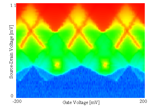 Figure 7. Current through a superconducting
single-electron tunneling transistor as a function of the gate voltage
and the bias voltage. The current is periodic in the gate voltage with
a periodicity of e/Cg, where e is the charge of
an electron and Cg is the gate capacitance. Blue corresponds
to nearly no current and red corresponds to a current of about 1 nA.
Many of the experiments carried out on artificial atoms have been performed
at low temperatures. This is because the characteristic energies of artificial
atoms depend on the size of the structure. These energies have to be larger
than the energies of thermal fluctuations in order for the atomic structure
to be observable. In real atoms the energy spacing between quantum levels
is typically a few electron volts (eV) while thermal the energy of a thermal
fluctuation at room temperature is 0.025 eV. Thus quantized energy levels
of real atoms are easily distinguished at room temperature. So far most
of the artificial atoms that have been made are relatively large and the
temperature where the atomic structure becomes apparent is rather low.
As advances in nanotechnology continue, the size of the structures will
decrease and the temperatures at which the atomic structures will be observable
will increase. This will open the way to room temperature applications.
Figure 7. Current through a superconducting
single-electron tunneling transistor as a function of the gate voltage
and the bias voltage. The current is periodic in the gate voltage with
a periodicity of e/Cg, where e is the charge of
an electron and Cg is the gate capacitance. Blue corresponds
to nearly no current and red corresponds to a current of about 1 nA.
Many of the experiments carried out on artificial atoms have been performed
at low temperatures. This is because the characteristic energies of artificial
atoms depend on the size of the structure. These energies have to be larger
than the energies of thermal fluctuations in order for the atomic structure
to be observable. In real atoms the energy spacing between quantum levels
is typically a few electron volts (eV) while thermal the energy of a thermal
fluctuation at room temperature is 0.025 eV. Thus quantized energy levels
of real atoms are easily distinguished at room temperature. So far most
of the artificial atoms that have been made are relatively large and the
temperature where the atomic structure becomes apparent is rather low.
As advances in nanotechnology continue, the size of the structures will
decrease and the temperatures at which the atomic structures will be observable
will increase. This will open the way to room temperature applications.
One of the most exciting areas of research is the possibility of coupling
artificial atoms together to form artificial molecules or they can be placed
in a regular pattern to form wires or crystals. A number of predictions
have been made for the electrical conductivity in such systems. Normally,
electrical conduction is governed by the motion of electrons that flow
like a liquid through a conducting material. As the electron liquid is
cooled, it can condense into a number of different quantum states. These
states include superconductivity, Luttinger liquids, magnetism, charge
density waves, spin density waves, and Wigner crystals. The type of condensed
state that is observed in a given material depends on the electron - electron
interactions in that material. The effects of electron - electron interactions
are intensified in quasi-one dimensional conductors such as molecular wires
and single rows of atoms on a substrate. The interactions are more important
in one-dimensional conductors because the diameter of the wire is smaller
than the effective radius of the conduction electrons. In that case, the
electrons cannot pass by each other and the motion of the electrons is
determined by the interactions. Using nanofabrication it is possible to
fabricate one-dimensional wires by a number of different means. Atoms can
be deposited in a row, or atoms can be pushed into a row with an STM, or
individual long conducting molecules can be attached to the electrodes.
The enhanced electron-electron interactions in these structures and the
condensed states they produce can then be explored by cooling the atomic
wires down. Work is continuing towards fabricating such quantum wires.
Figure 8 illustrates the sort of control that has presently been achieved.
The lines in the figure are only a few atoms wide.

Figure 8. The closely spaced vertical lines are rows of atoms on a silicon surface. The modification of the surface was done with an STM. (Sven Rogge, Delft University of Technology).