Electrochemical Growth of Organic Conducting Microcrystals of Tetrathiafulvalene Bromide
Marta Mas-Torrent, * Peter Hadley,
Kavli Institute of NanoScience, Delft University of Technology, Lorentzweg 1,
2628 CJ Delft, The Netherlands, Fax: (+31) 1527-83251
email: Marta Mas-Torrent (marta@qt.tn.tudelft.nl)
Correspondence to Marta Mas-Torrent, Kavli Institute of NanoScience, Delft University of Technology, Lorentzweg 1, 2628 CJ Delft, The Netherlands, Fax: (+31) 1527-83251
M. M.-T. thanks the Generalitat de Catalunya for a Nanotechnology
fellowship. The authors also thank Prof. C. Rovira for useful
discussions.
| Keywords |
| charge transfer • conducting materials • electrochemical methods • molecular electronics • nanowires |
| Abstract |
 |  | |
| No Abstract |
Received: 26 January 2005
| Digital Object Identifier (DOI) |
10.1002/smll.200500034 About DOI
| Article Text |
A new trend in electronics research is to increasingly employ chemical synthesis techniques in order to fabricate device components exhibiting physical properties addressed to specific applications. Examples of this approach are circuits made from carbon nanotubes and semiconducting nanowires.[1] These nanostructures can be used, for instance, as chemical or biological sensors.[2] In addition, chemical synthesis can be scaled up easily, which could give rise to cheaper devices. In this respect, it is interesting to consider nanowires or microwires of conducting organic salts as an appealing alternative route for the fabrication of nanoscale devices. In this paper, we describe the preparation of very good quality microcrystals of the metallic organic charge-transfer salt, tetrathiafulvalene bromide ((TTF)Brx).[3] The methodology employed here allows for the controlled synthesis of large quantities of microcrystals and could also be extendable to the fabrication of a multitude of charge-transfer salts with different physical properties.
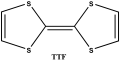
In the field of organic conductors, the development of new organic charge-transfer salts based on tetrathiafulvalene (TTF
 | [Normal View 3K | Magnified View 4K] |
 ,8,8-tetracyanoquinodimethane (TTF-TCNQ) over thirty years ago.[4]
Since then, a wide range of TTF salts, typically synthesized by
electrocrystallization means and showing an extensive variety of
electrical properties (e.g. semiconducting, metallic, and
superconducting), has been prepared.[5] An
additional attractive feature of these salts is the possibility of
preparing materials in which electrical, magnetic, and optical
properties can coexist.[6]
,8,8-tetracyanoquinodimethane (TTF-TCNQ) over thirty years ago.[4]
Since then, a wide range of TTF salts, typically synthesized by
electrocrystallization means and showing an extensive variety of
electrical properties (e.g. semiconducting, metallic, and
superconducting), has been prepared.[5] An
additional attractive feature of these salts is the possibility of
preparing materials in which electrical, magnetic, and optical
properties can coexist.[6]Despite the intense work focused on preparing a large range of TTF salts, little attention has been paid to obtaining microcrystals of these salts. Films of metallic and semiconductor microcrystals embedded in polymeric matrices have been prepared by treating a film containing the TTF derivative with vapors of an oxidant reagent.[7], [8] Jeszka et al. have reported different methods for obtaining microcrystals of ET2I3 (ET stands for bis(ethylenedithio)tetrathiafulvalene) by recrystallization or by treating the ET microcrystals with iodine vapors.[9] However, these methods are limited to particular materials and, for a general applicability, the use of electrocrystallization techniques is required.[10] Fabrication of microcrystals of the charge-transfer salt (TTF)Brx grown electrochemically was previously achieved on a graphite surface catalyzed by platinum nanoparticles.[11] Here we have employed two new methodologies to grow (TTF)Brx microcrystals electrochemically. The first method combines both bottom-up and top-down approaches, involving the growth of microcrystals from their precursor molecules on electron-beam-patterned gold microlectrodes. Interestingly, this method gives rise to the production of a large amount of conducting microcrystals. The second strategy allows for the fabrication of microcrystals on an insulating SiO2 surface. Thin layers of SiO2 are good insulators for electron transport but allow an ion current to pass through them. This makes it possible to grow crystals electrochemically on an electrically insulating substrate. Such a process could be attractive for the preparation of electronic devices where SiO2 substrates are typically employed.
The setup used in our first approach is illustrated in Figure 1. The prefabricated microelectrodes (4 nm of Ti, acting as a sticking layer, covered by 26 nm of Au) were fabricated by electron-beam lithography on a silicon wafer with a 200-nm-thick thermally grown oxide layer and with a double layer of poly(methyl methacrylate) as resist. Five microliters of a 0.1 M solution of tetrabutylammonium bromide (TBABr) and 5 mM of TTF in dimethylacetamide were placed on the prefabricated electrodes. The electrochemical experiments were performed by coupling a potentiostat to a Microscope Probe Station. A gold needle in contact with one of the prefabricated gold electrodes was used as a working electrode and two platinum wires were used as counter and pseudo-reference electrodes. The application of a series of 20 voltage pulses of 0.4-0.6 V vs. Pt with a duration of 0.2 s resulted in the electrochemical growth of microcrystals on the working electrode. The samples were then rinsed with ethanol and carefully dried under a flow of nitrogen. Under these experimental conditions, the product of the oxidation is known to be the nonstoichiometric salt (TTF)Brx, where x is close to 0.76.[3]
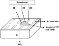 | Figure 1. Schematic
drawing of the experimental setup. The abbreviations WE, RE, and CE
stand for working electrode, reference electrode, and counter
electrode, respectively. [Normal View 7K | Magnified View 13K] |
Figure 2 shows scanning electron microscope (SEM) images of the (TTF)Brx
crystals grown on the prefabricated gold electrodes. Long, thin
crystals with smooth surfaces and well-defined faces are obtained. On
average, the crystals prepared are 1-2  m long and about 200 nm wide. (TTF)Brx crystallizes by forming
  -stacks of TTF/TTF+ along the c axis of the crystal arranged parallel to rows of Br-.[3]
The mixed-valence character of this salt, together with the electron
delocalization along the stacking direction, leads to conducting
crystals along the c axis. Thus, during the electrocrystallization the (TTF)Brx crystals grow preferentially along c, resulting in long, narrow crystals.
-stacks of TTF/TTF+ along the c axis of the crystal arranged parallel to rows of Br-.[3]
The mixed-valence character of this salt, together with the electron
delocalization along the stacking direction, leads to conducting
crystals along the c axis. Thus, during the electrocrystallization the (TTF)Brx crystals grow preferentially along c, resulting in long, narrow crystals.
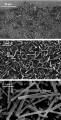 | Figure 2. SEM images of (TTF)Brx
microcrystals grown electrochemically and on prefabricated gold
electrodes, shown (top to bottom) with increasing magnification. [Normal View 130K | Magnified View 322K] |
The second variant of the electrochemical experiment was carried out by using a silicon wafer with only an 8-nm-thick SiO2 layer. Gold nanoparticles were deposited from solution onto the SiO2 surface prior to the electrochemical experiment. The growth of the (TTF)Brx microcrystals was carried out as described previously but using the Si substrate as the working electrode. Pulses of 4 V (versus Pt) of 0.2 s duration were applied. Although in this case the working electrode is not in contact with the electrolyte solution, due to an ionic leakage current through the SiO2 dielectric, (TTF)Brx microcrystals grew on the SiO2 surface predominantly from the deposited gold particles, which act as nucleation points (Figure 3).
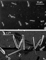 | Figure 3. SEM images of (TTF)Brx microcrystals grown electrochemically on a silica substrate, with gold nanoparticles acting as nucleation points. [Normal View 61K | Magnified View 154K] |
The electrical properties of a single microcrystal were measured on the prefabricated electrodes. Figure 4 shows the current-voltage characteristics of one (TTF)Brx crystal placed between gold source and drain electrodes 5 m
apart. An SEM image of the measured crystal is shown in the inset of
this figure. The crystal exhibits a resistance of 20 M .
A plot of the source-drain current at a source-drain voltage of
0.5 V while sweeping the gate voltage applied to the Si substrate
is also shown in the inset of Figure 3. No clear gate-effect is observed, which would be expected for a metallic material.
.
A plot of the source-drain current at a source-drain voltage of
0.5 V while sweeping the gate voltage applied to the Si substrate
is also shown in the inset of Figure 3. No clear gate-effect is observed, which would be expected for a metallic material.
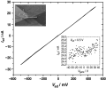 | Figure 4. Source-drain current (Isd) versus source-drain voltage (Vsd) for a (TTF)Brx crystal placed between two prefabricated gold electrodes 5 m apart. Insets: SEM image of the measured device and plot of the Isd dependence versus the gate voltage at Vsd=0.5 V. [Normal View 16K | Magnified View 31K] |
In conclusion, we have reported the electrochemical synthesis of large quantities of microcrystals of the conducting charge transfer salt (TTF)Brx on gold microelectrodes and on a silica substrate using gold nanoparticles as crystalline nucleation points. This technique could be extendable to the preparation of a vast number of charge-transfer salts and, therefore, organic microcrystals with a large variety of electrical properties or even combining different physical properties could be accessible. The controlled fabrication of microcrystals with specific electrical properties represents a step forward in the chemical synthesis of electronic components.
 | | |
Tetrathiafulvalene
(TTF; >98 %), dimethylacetamide (99 %), and
tetrabutylammonium bromide (TBABr; 99 %) were purchased from
Aldrich and were employed without further purification. A solution of
gold nanoparticles of diameter 250 nm was purchased from Ted Pella
Inc. The electrochemical experiments were carried out with a Autolab III potentiostat coupled to a Karl S³ss Microscope Probe Station.
The electrode fabrication was carried out with an electron-beam pattern generator (EBPG5 HR 100 kV FEG) using a double poly(methyl methacrylate) resist. Four nanometers of Ti and 26 nm of Au were evaporated at liquid-nitrogen temperature to ensure a smooth surface; lift off was done in warm acetone. The samples were then rinsed with isopropanol and dried under nitrogen.
The samples were inspected with a scanning electron microscope (Philips XL30SFEG).
| References |
| | |