1. Introduction
Over the years, the lateral dimensions in microelectronic circuits
have been shrinking systematically by a factor of two every six years.
The extrapolation of the past, formulated in Moores law, serves as the
prescription for the future as laid down in the Roadmap for the Semiconductor
Industry. [1] This Roadmap indicates gate widths for CMOS transistors of
35 nm in the year 2012. Continuation would predict minimum feature sizes
of 1 nm around 2040. Many times in the past a breakdown of Moores law
has been predicted, due to limitations in fabrication, excessive power
density or discontinuous change of physical behavior. So far, the impetus
of the collective microelectronics industry has pushed aside such obstacles
with remarkable ease. Nevertheless, it is hard to imagine silicon CMOS
technology on the true nanometer scale. Will new quantum nanodevices take
over? Many introductions to papers on quantum devices suggest that this
will be the case. In this chapter, we attempt to analyse the long term
potential for microelectronics applications of quantum devices. Obviously,
this analysis can only depart from the types of devices and from the physics
effects that we know of today. We will limit ourselves to electronic transport
devices. We focus strongly on devices that are based on manipulation of
single electrons.
Quantum devices can be made of many materials and be based on various physical principles. However, they share common properties. The relevant energy levels for their operation can be estimated, also for devices that in future would make use of perfect fabrication at the atom by atom level. Quantitative estimates will be given for the performance as switches and memory cells in digital applications at various temperatures. The conclusion will be that quantum devices are unlikely to replace CMOS technology in computers of the types that we know today. Future developments that involve new and different physics effects may change the picture. It may also be that quantum devices can be used in drastically different modes of operation, where the quantum coherence extends over multiple elements. An extreme example is so called quantum computation, where the whole computer is one coherent quantum system and information is processed in a way that has no analogy with the classical Turing-type computer. We will briefly indicate the principles of quantum computation and discuss the merits of solid state quantum devices for this purpose.
Warnings against unfounded optimism about the potential for application of quantum devices in microelectronics have been sent out repeatedly by Landauer. Titles such as: Need for Critical Assessment [2] and Is Quantum Mechanics useful? [3] speak for themselves.
2. General physics aspects
In quantum devices, the addition or extraction of a single electron
significantly changes the energy of the system. For those devices that
are fabricated lithographically with sizes down to tens of nanometers,
the energy change is small compared with room temperature and devices have
to be cooled down. Future controlled atom by atom fabrication techniques
may allow the production of quantum devices with dimensions around one
nanometer. Here, as we will see, the energy changes may be up to thirty
times room temperature. It is necessary to confine the electrons to a well-defined
region i.e. the molecule, the quantum dot, the cluster or the metallic
island. Electronic wave functions may only be weakly coupled to the outside
world. The main effects are based on two energies: the Coulomb charging
energy for one additional electron and the particle-in-box confinement
energy. General background to the physics issues that are discussed here
are found in references [4] and [5].
CHARGING ENERGY
The Coulomb charging energy will be indicated as EC
is this chapter. It is equal to e2/2CS,
where e is the electronic charge and CS
is the sum of the capacitances between the element considered and all other
elements and conductors, including the self-capacitance to the far-away
ground. A sum capacitance of 1 aF (attofarad = 10-18 F) yields
a charging energy of 80 meV or 900 K. For a flat disk of diameter D
(expressed in nm) surrounded by a dielectric with relative permittivity
e, the self-capacitance in attofarads is approximately
0.04eD. The contribution from the connecting
leads and gates has to be added. The conclusion is that with extreme nanofabrication
a capacitance of 0.1 aF and a charging energy of 1 eV or 10,000 K might
be obtainable. This statement might be misleading without the following
addition: for error-free operation at the level of digital computing the
temperature should stay below the energy by at least a factor 30. At this
time, controlled fabrication of elements that can be used in a circuit
allows for a charging energy of around 10 meV or smaller.
CONFINEMENT ENERGY
The two lowest energy levels for a particle with effective mass m*
in a one-dimensional square box of width w, are separated by an
energy 3h2/(8em*w2). This is equivalent
to about (mo/m*) (1 nm/w)2 eV.
For electrons in semiconductors mo/m* can be of
order 10, but for devices that are not large compared with the lattice
constant, this advantage is lost as the band concept breaks down. With
extreme nanofabrication one expects that the highest obtainable confinement
energy will be around 1 eV, similar to the highest charging energy.
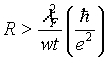
TUNNEL BARRIERS
Transport in and out of the quantum elements is needed for operation,
but the electronic states should not be mixed with external states. To
achieve the isolation of electronic states, tunnel barriers are used. The
electronic levels are well-defined when the tunnel resistance is much higher
than the quantum resistance Rq=h/e2 (h
is Plancks constant), or 25 kW. The quantum
effects are smeared out or lost with more transparent tunnel barriers.
This is most easily made plausible for the charging effects, where the
Heisenberg uncertainty time connected to a charging energy EC
is h/(2pEC)=hC/(pe2).
For shorter times no control is possible. Typical operation times are of
order RC, which leads to the requirement R>>Rq.
For confinement a similar reasoning, equally fundamental of character,
applies. The unavoidable consequence is that impedance levels in quantum
circuits are of order 100 kW or higher. Barrier
heights can sometimes be made tuneable, so that retention times can be
long in combination with reasonable switching times.
ENVIRONMENT
The dynamical response of quantum devices is strongly determined by
their electromagnetic environment. The environment includes degrees of
freedom such as phonons when they couple to electromagnetic phenomena.
Transitions that are otherwise forbidden can occur when additional or missing
energy can be dumped into or drawn from certain environmental modes (an
ohmic reservoir can be modeled by a large number of harmonic oscillators
with a wide range of frequencies). When transport between quantum elements
is coherent, no simple addition applies. In the design of quantum circuits
with multiple elements, close attention needs to be paid to these aspects.
Their overall effect may be increases of operating time, impedance and
required volume.
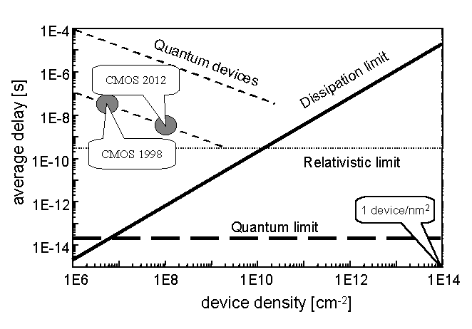
3. Physical limits of integrated circuits
As computers are made faster and cheaper, the dimensions of the transistors
that make up the integrated circuits have decreased. This allows ever more
transistors to be crowded on a computer chip. While more transistors have
been added to a chip, the price of producing one square centimeter of integrated
circuit has remained constant at roughly $100. [1] If the economies of
scale continue to operate as they have in the past, the way to continue
to make computers even more cheaply is to make even smaller transistors
and crowd them more densely on a chip than they have been in the past.
This will push the circuits into the realm of mesoscopic physics, where
quantum mechanics determines the behavior of the circuits.
If the price per square centimeter of an integrated circuit remains
constant, then an appropriate figure of merit for comparing different technologies
is the number of operations that are performed per square centimeter per
second. Even if the price per square centimeter does not remain constant,
it is likely that in the future microprocessors will have an area of a
few square centimeters. Larger integrated circuits will be unwieldy and
making smaller processors will limit their capabilities. Thus it is interesting
to know how much computing power can be packed in a square centimeter.
There are two ways to increase the computing power of an integrated circuit,
either the device density can be increased or the delay time associated
with an operation can be decreased. In Fig. 1 the device density is plotted
versus the average delay per device. The average delay per device is often
much less than the clock frequency because not every device switches every
clock cycle. The average delay depends on the circuit architecture. It
is not possible to increase the density or decrease the average delay without
bounds.
DISSIPATION LIMIT
One of the most important limitations is formed by the dissipation
of heat that is generated by the circuit. Integrated circuits that are
not actively cooled typically operate at a temperature about 100 C and
give off heat to the room temperature environment. At this temperature,
typical thermal fluctuations have an energy of kBT =
5 × 10-21 J. In order for a bit to be stable against thermal
fluctuations, the energy needed to flip a bit must be at least 10 times
a typical thermal fluctuation or 5 × 10-20 J. If quantum
computing and reversible computing schemes are ignored for the moment,
at least 5 × 10-20 J is dissipated for each operation
the integrated circuit performs. The power dissipated per square centimeter
by an integrated circuit is therefore at least the device density times
the number of operations per second per device. In real microprocessors
the dissipation is considerably more than this. The amount of thermal energy
that can be transported away from the circuit is limited by the thermal
conductivity of the environment of the circuit. The amount of power that
can be typically transported away from the circuit is 25 W/cm2.
[1] This dissipation limit is plotted on the density delay diagram of
Fig. 1. If we assume that the average cost of a square centimeter of integrated
circuit remains constant, then the number of operations performed per second
per unit cost can be drawn as a line in Fig. 1. that is parallel to the
dissipation limit. The technology that comes the closest to the dissipation
limit will deliver the most computational power per unit cost.
QUANTUM FLUCTUATIONS
Quantum fluctuations can also disrupt circuit performance. According
to Heisenbergs uncertainty principle, a quantum fluctuation of energy
E can occur for a time h/E.
If the energy necessary to flip a bit is greater than 5 × 10-20
J to make the circuit stable against thermal fluctuations, then quantum
fluctuations will occur for times less than 2 × 10-15
s. For the circuit to be stable against these quantum fluctuations, the
switching time of a device should be at least 10 times longer than a quantum
fluctuation. This means that switching times must be longer than 2 ×
10-14 s. The quantum limit intersects the dissipation limit
at a density of 107 devices/cm2. This is about the
current device density of CMOS. This leads to the conclusion that no dissipative,
room-temperature general-purpose computation scheme with a device density
greater than CMOS circuits will be quantum noise limited. Quantum fluctuations
become more relevant in cooled circuits and high speed signal processors.
RC DELAY
One of the factors that limits the speed of integrated circuits is
the RC delay. When a particular node in a circuit is charged, the delay
is the total capacitance of the node times a resistance through which the
node is charged. The resistance is the sum of the output impedance of the
device charging the node and the resistance of the wire leading to the
node. In CMOS circuits, much attention has recently been given to the increase
of the RC time due to the resistance of the wire leading to the node. This
resistance increases as all dimensions of a wire are scaled down. The formula
for the resistance of a diffusive wire is
 ,
[1]
,
[1]where r is the resistivity, l is the length, w is the width, and t is the thickness. If l, w, and t are all decreased by a certain factor, the resistivity R increases by the same factor. An increase in R slows down the circuit. This situation gets even worse for very short wires. As the length of a wire goes to zero, the resistance does not go to zero as Eq. 1 predicts. The resistance of the wire is always limited by the relationship [6]
 .
[2]
.
[2]Here lF is the Fermi wavelength. This means that there is a critical length, below which Eq. 1 is no longer valid,
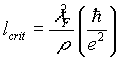 .
.For metals this critical length is about 10 nm. One expects an increase in the resistance when the distance between devices approaches 10 nm.
For quantum devices such as single-electron transistors and quantum dots, the dominant resistance is not the wire that connects the nodes; it is the output impedance of the device itself. The output impedance of a single-electron transistor or a quantum dot must be greater than the resistance quantum. This means the resistance that determines the delay is roughly 1000 times larger in a quantum circuit than in CMOS. The way to compensate for this increase in resistance is either to decrease the capacitance of the nodes or to increase the packing density so that more computational elements are packed in a square centimeter. The capacitance of the nodes is largely determined by the physical size of the components of the circuit. This means that for the same device density, high resistance quantum devices are going to be slower than CMOS. This is reflected in the position of the quantum devices in Fig. 1. As long as a low impedance element like a field-effect transistor can be used for logic circuits it will be used because the resulting circuits will be much faster.
RELATIVISTIC LIMIT
Another limit that has consequences for integrated circuits is the
relativistic limit that is caused by the finite speed of light. No information
can be transported a distance of 1 cm in less than 0.3 ns. It is possible
for integrated circuits to operate in the relativistic regime but if the
average delay is to be much less than the relativistic limit, the circuit
must be designed such that most of the communication between devices is
local. The shorter the delay, the more local the communication must be.
In Fig. 1 the relativistic limit was drawn for a circuit with an area of
one square centimeter. For larger circuits, the limit will have a longer
average delay time.
4. Single-Electron Transistors
Although a number of different quantum devices could be used to build
circuits, the quantum device that has been most widely discussed is the
single-electron transistor (SET). [7] A single-electron transistor is a
three terminal device consisting of an input terminal (the gate) and two
output terminals (the source and drain). A change in the charge on the
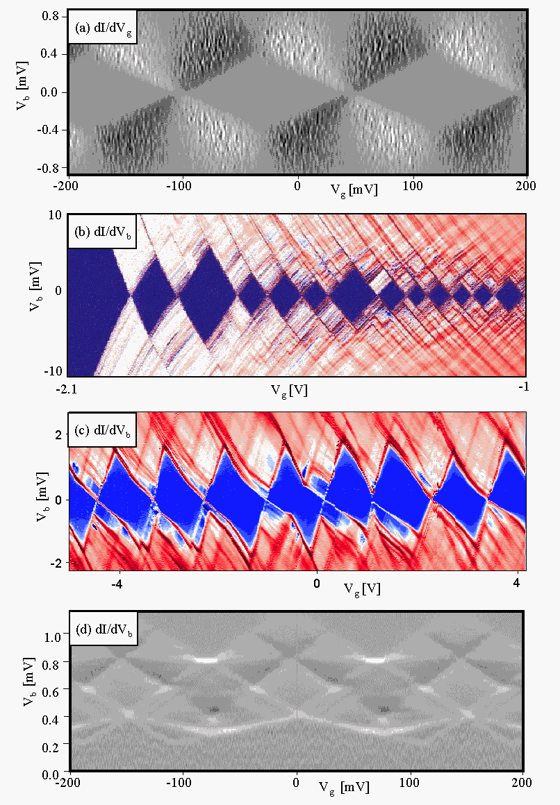
gate modulates the current that flows from source to drain. Figure 2 shows
the conductance through a SET as a function of bias voltage and gate voltage
for a metal SET, a semiconducting SET [8], a carbon nanotube SET [9], and
a superconducting SET [10]. For the metal SET and the superconducting SET,
the current that flows from source to drain is a periodic function of the
gate voltage with periodicity e/Cg, where Cg
is the gate capacitance. For the semiconducting SET and the carbon nanotube
SET, the current is not strictly a periodic function of the gate voltage.
This is because energy needed to add an electron to the island is the sum
of the charging energy and the confinement energy. For the semiconducting
SET and the carbon nanotube SET the charging energy has the same order
of magnitude as the confinement energy whereas the for a metal SET or a
superconducting SET the charging energy is much larger than the confinement
energy.
From the current-voltage characteristics one can determine that the input capacitance at the gate can be very small, typically 1 10 aF, and that there is virtually no input current leakage. The output impedance of a SET is quite large, typically 100 kW 100 MW. This is orders of magnitude higher than typical semiconductor devices. This causes the longer RC delay for SETs and quantum dots which was discussed above.
The data in Fig. 2 can also be used to determine the charge gain and the voltage gain of a SET. The charge gain is frequency dependent and determines the maximum operation frequency of the SET. When the gate charge is modulated with an amplitude Dq at a particular frequency, the current through the SET transistor is modulated with an amplitude DI at the same frequency. The charge that is transported through the SET transistor every half period is DIT/2, where T is the period. The charge gain is thus gq = DIT/(2Dq). In any circuit where the output of one SET drives the input of the next SET the charge gain has to be greater than one at the operating frequency. This is equivalent to saying that the gate must be modulated with a frequency much less than the average time between electron tunnel events e/I.
Voltage gain is necessary for some applications. The voltage gain of a SET is the ratio of the modulation of the source-drain voltage to the modulation of the gate voltage at a given current bias gv = DVDS/DVg. The voltage gain can be determined from the data in Fig. 1. The gain is gate voltage dependent and for small signals ranges between gv = -Cg/Cj and gv = Cg/(Cg + Cj). Voltage gain greater than one is only possible when the gate capacitance is greater than the junction capacitance. As an amplifier, a SET has a limited dynamic range. The gate charge modulation must be smaller than about e/3 for the small signal limit to apply. In the limit of large gate modulation, the voltage gain goes to zero.
The charge sensitivity of a SET is exquisite. Charge variations much
smaller that the charge of an electron can be detected. A typical charge
sensitivity for a SET is 10-4 e/![]() .
At this time, the SETs with the largest bandwidth are RF SETs which can
operate up to about 1 GHz [11]. The tremendous charge sensitivity of a
SET also introduces complications. A SET is so sensitive that it responds
to minute changes in the charge distribution of its environment. If a crystal
defect in the vicinity of a SET carries a charge e and moves slightly,
this will be detected by the SET. These charged defects are called background
charges or offset charges. [12] Even when the charged defects do not move,
they couple charge to the SET in the same way that the gate voltage does.
Thus offset charges produce a random shift along the gate voltage axis
of the current-voltage characteristics shown in Fig. 2.
.
At this time, the SETs with the largest bandwidth are RF SETs which can
operate up to about 1 GHz [11]. The tremendous charge sensitivity of a
SET also introduces complications. A SET is so sensitive that it responds
to minute changes in the charge distribution of its environment. If a crystal
defect in the vicinity of a SET carries a charge e and moves slightly,
this will be detected by the SET. These charged defects are called background
charges or offset charges. [12] Even when the charged defects do not move,
they couple charge to the SET in the same way that the gate voltage does.
Thus offset charges produce a random shift along the gate voltage axis
of the current-voltage characteristics shown in Fig. 2.
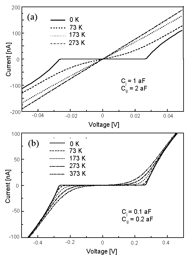
For circuits to operate properly, the charging energy should be much greater than the thermal fluctuations. At 373 K, the charging energy equals kBT for a capacitance of 2.5 aF. However simulations show that there is hardly any modulation of the current for a SET with CS = 2.5 aF at 373 K. It is necessary to have junction capacitances of about 0.1 aF before significant current modulation is achieved. Figure 3 shows a simulation of the current-voltage of a SET with junction capacitances of 1 aF and 0.1 aF and a modest voltage gain of 2. These capacitances are extremely small and correspond to islands only a few nanometers in size. It will be impossible to make the SETs much smaller than this because SETs or quantum dots that operate at room temperature will only be a few atoms wide. This means that there will not be much opportunity to scale room-temperature SETs smaller once they are fabricated.
The switching delay of a SET can be much longer than the RC delay explained above. This occurs at high temperatures where the current modulation of a SET decreases from the maximum low temperature value of approximately e/(RCS). This also occurs for multiple tunnel junctions where random offset charges reduce the current modulation to below the optimum value even at low temperature. In these cases, the minimum delay time is the inverse of the maximum frequency for which there is charge gain, f = DI/e.
5. Applications
LOGIC
SETs dissipate little power and can be fabricated in sizes ranging
down to a molecular scale. These characteristics make them potentially
useful for logic and memory circuits. It has been suggested that large-scale
integration of single-electron transistors could result in logic circuits
with a high device packing density. Recently a number of different logic
schemes using single-electron-tunneling transistors have been proposed.
[13]
In single-electron logic (SEL) proposed by Averin and Likharev, bits are represented by individual electrons. [14] SEL has an architecture similar to superconducting single flux quantum logic where individual magnetic flux quanta are manipulated. [15] A logic scheme where bits were represented by individual electrons was also proposed by Ancona. He proposed building circuits with a regular cellular structure with local connections as in cellular automata. [16] Tucker [17] and Yoshikawa et al. [18] suggested the use of single-electron transistors in an architecture very similar to CMOS. In this case the bits are represented by voltage levels. [19, 20] The use of multiple tunnel junctions in place of individual single electron transistors in this sort of architecture has also been proposed. [21] Tougaw and Lent suggested that the electron configuration in a cluster of quantum dots could be used to encode the information. [22] The clusters of quantum dots are placed very close together but they are not electrically connected. The information passes from one cluster to the next via the Coulomb interaction between the electrons. Computation proceeds locally as in a cellular automata architecture. Korotkov proposed a similar computational scheme using clusters not connected by wires. [23] Unlike Tougaw and Lent, Korotkov suggested the use of an ac driving field so that the energy needed to drive the computation could be coupled into each of the clusters directly. Ohshima and Kiehl also proposed a SET logic scheme using an ac pump (tunneling phase logic). [24] In this scheme the information is not coded in the configuration of some charge on a cluster but it is coded in the relative phase between the ac pump and the periodic single-electron tunneling oscillations. Likharev and Korotkov also proposed reversible logic elements [25] where the amount of energy dissipated per switching event could be much less than kBT. There have also been several suggestions to use single-electron tunneling transistors to build neural nets. Goossens et al. suggested exploiting the periodic transfer characteristics of a SET transistor to build neural nets [26] while the quantum neuromorphic networks of Bandyopadhyay et al. [27] function more like a traditional Hopfield machine.
Although many logic schemes have been proposed, very few circuits have been tested experimentally. Recently a simple SET logic circuit, which displays negative differential resistance, was demonstrated using a multilayer fabrication technology. [28] A multilayer fabrication technology is important since wires must cross in complex circuits. The negative differential resistance device was constructed from two SETs with a voltage gain greater than 1. Voltage gain is required in many of the logic schemes mentioned above.
No logic scheme based on quantum devices is presently threatening to overthrow the semiconductor industry standard CMOS technology for logic applications. Many of these logic schemes are flawed in that they ignore the existence of offset charges. This is unrealistic. There is no experimental evidence that offset charges can be eliminated in any materials system. The only offset-charge independent logic schemes use high resistance resistors. However fabricating suitable compact, low capacitance, high resistance resistors is a formidable technological problem. Even if this were to be achieved, the high resistance make the quantum devices so much slower than CMOS that they are not competitive.
QUANTUM COMPUTATION
So far, we have discussed the possible replacement of CMOS semiconductor
elements by quantum devices. Their role in the circuit would be identical.
It turned out that quantum devices provide no major advantage in this conventional
setting. Much more might be gained if the intrinsic coherence of quantum
states is used. The evolution in time of an isolated quantum system under
the influence of a known external drive is completely deterministic. Quantum
uncertainty comes in when a measurement is performed; i.e. the quantum
system is made to interact with a large number of uncontrolled classical
variables. Quantum devices in a classical matrix are continuously subjected
to a measurement in this sense, resulting in severe limitations in performance
due to quantum fluctuations.
Quantum systems can exist in general superpositions; for a two level system, the relative amplitude and the relative phase of the occupation coefficients are two independent continuous variables. In principle, these variables can be manipulated, in particular by the application of microwave pulses of the frequency that corresponds to the energy difference between the two states. Two-level quantum systems can also be coupled, so that their states are entangled. There is no classical analogue to the notion of quantum entanglement.
In the last few years the principles have been worked out for a new method of information processing that is called quantum computation. [29] In a quantum computer of this type, the bits are replaced by qubits (two level systems as described in the previous paragraph). Qubits can be coupled by quantum gates. The whole quantum computer with N qubits lives in a superposition of its 2N quantum states. The applied operations correspond to a unitary transformation that has to be expressed by a 2N by 2N matrix. For a computation, the quantum computer is first prepared in a known state and a series of operations is performed. Finally a measurement is performed; that destroys the quantum information. During the computation no decoherence due to coupling to external degrees of freedom is allowed.
It has been shown that a quantum computer can perform certain tasks much faster than a CMOS computer. A good example is the factorization of a large number: the time needed to factorize a number of N digits increases exponentially in a conventional computer but only with a power law in the quantum computer. [30] Quantum coherence brings in an essential advantage. To be competitive, a quantum computer needs a minimum of 104 or 105 qubits and a comparable number of operation steps, all performed within the decoherence time.
Only rudimentary quantum computers of a few qubits have been realized so far by means of nuclear magnetic resonance and by laser manipulation of electron states in trapped single atoms. Integration to large numbers of qubits seems difficult. The use of solid state quantum devices of the types described in this book can be considered. Ideas concentrate mostly on spin polarized states in quantum dots and charge or fluxoid states in circuits of superconducting tunnel junctions. The suitability is mainly determined by the effective decoherence rate. Decoherence times that have been measured are in the order of 1 ns, in situations where measuring leads are connected and for systems that are susceptible to charge noise. For optimized devices much longer times, more than 1 ms, are calculated. Certainty can only be obtained from experiments. If solid-state quantum devices demonstrate sufficient coherence, the fact that they can be integrated into large circuits makes them excellent candidates for the development of a real quantum computer.
MEMORIES
Memories are a more promising application of quantum devices than logic
because density is more important for memories and speed is less important.
Although great advances have been made in computer memories, there remains
much room for improvement. The density of a two dimensional memory is ultimately
limited by the thickness of the address lines to the memory cells. The
thinnest conductors that conduct over long distances are about 1 nm wide.
This would result in a density of about 1013 bits/cm2.
Such a memory would have a linear information density about equivalent
with DNA.
In single-electron memories, a bit is represented either by one electron or a few electrons on a storage node. The basic memory cell also has a charge-sensing device, either a field effect transistor or a single-electron transistor. The charge-sensing device has to exhibit charge gain. The speed of these memories is limited by the time it takes to charge and discharge the storage node and by the maximum frequency for which the charge-sensing device exhibits charge gain. Yano et al. [31] and Stone et al. [32] used naturally occurring grains as the storage nodes and a chain of naturally occurring grains to sense the charge. There is no control of the structure of the grains, which leads to some parameter spread but grains can be small enough that effects are observable at room temperature. Guo et al. [33] also achieved room temperature operation using a single artificially structured polysilicon dot as the storage node and a field effect transistor as the charge-sensing device. Likharev discussed memory cell where the charge-sensing device is a SET and has critically examined the optimal parameters of the tunnel barrier that is used to charge the storage node. [34]
METROLOGY AND SENSORS
Quantum devices seem certain to make a major contribution to the field
of precision measurements and charge sensors. Single-electron transistors
are the most sensitive charge measurement devices presently available.
A SET is in many respects the dual to the SQUID, the superconducting sensor
of magnetic flux. In a SQUID, a so-called flux transformer can be used
to separate the sensor and the pick-up coil. No such possibility exists
for the SET. A long lead to the gate implies a large capacitance that is
added to the total island capacity and destroys the sensitivity. Consequently,
the SET has to be brought in the direct neighborhood of the potential to
be measured. A natural and very interesting solution is to position the
SET on the tip of a scanning probe system. This has first been realized
by Yoo et al. [35]. When a single-electron transistor is fabricated on
the tip of a scanning probe, it is possible to use the tip as a STM or
AFM to determine the topology, while the SET measures potential variations.
The sensitivity at room temperature should ultimately be high enough to
detect single electron charges with a spatial resolution in the sub-nm
scale.
Single-electron devices can also be used to make precise measurements of current. A device related to a SET is an electron pump. In an electron pump, gates are modulated to repeatedly push individual electrons through a circuit. This produces a current with a magnitude I = ef, where I is the current and f is the modulation frequency. An inaccuracy of 10-8 has been reached by Keller et al. [36]. For metrological applications, low temperatures are not a strong disadvantage. However, nanoscale devices with much smaller capacitance will be extremely useful as the operating frequency can be brought to a level that corresponds to more reasonable current levels (100 GHz corresponds to only 16 nA).
7. Conclusions
It is very unlikely that single electron quantum devices will replace
CMOS as switching elements for logic in general purpose computation. The
main disadvantage is the intrinsically high impedance level of more than
100 kW. If the product of device impedance and
interconnect capacitance determines the response time, with equal interconnect
lengths the lower impedance device wins. Drastically new ideas would be
needed for this conclusion to be changed. In the area of memories, where
raw speed is less important, single-electron quantum devices may eventually
be competitive.
Single-electron quantum devices can only be used for regular computation at room temperature when their dimensions are below 10 nm. Controlled fabrication for large circuits will not come available until the microelectronics Roadmap dictates this. Clearly 10 nm is getting so close to the finally unavoidable end of the road, that the willingness to make a switch to a completely new technology may not exist, even when the performance of quantum devices would be superior.
Nanoelectronics based on quantum devices may be relevant for applications that are complementary to standard information processing, rather than competitive. The low power level of quantum devices make them highly suitable for fault-tolerant computation at very high densities. A local architecture will be needed to avoid long delay times due to the high resistance.
Predictions about the long-term potential of new types of devices may
well be wrong, as they are subject to the limitations of our present imagination.
The field of quantum devices is young and new ideas may provide a breakthrough.
Quantum computing is an example that makes essential use of the quantum
character without any classical analogue. Even if quantum devices do not
replace mainstream semiconductor devices, the continued study of quantum
effects that occur on a nanometer length scale is important because these
effects will influence the performance of CMOS semiconductor devices when
they reach the nanometer regime.
Acknowledgments
This research was supported by CHARGE, Esprit project 22953, NEDO, and by Stichting voor Fundamenteel Onderzoek der Materie (FOM).
References
1. The National Technology Roadmap For Semiconductors, Semiconductor
Industry Association, (1997). http://notes.sematech.org/ntrs/PublNTRS.nsf
2. R. Landauer, IEEE Trans. Electron Devices 43, 1637 (1996).
3. R. Landauer, Philos.Trans.R.Soc.London, Ser.A 353, 367 (1995).
4. Single Charge Tunneling, edited by H. Grabert and M.H. Devoret,
Plenum Press, New York, (1992).
5. Mesoscopic Electron Transport, edited by L.L. Sohn, L.P.
Kouwenhoven and G. Schön, Kluwer Academic Publishers, Dordrecht, (1997).
6. Y. V. Sharvin, Sov. Phys. JETP 21, 655 (1965).
7. K. K. Likharev, IEEE Trans. Mag. 23 1142 (1987).
8. L.P. Kouwenhoven, T.H. Oosterkamp, M.W.S. Danoesastro, M. Eto, D.G.
Austing, T. Honda, and S. Tarucha, Science 278, 1788 (1997).
9. Sander J. Tans, Michel H. Devoret, Remco J.A. Groeneveld, and Cees
Dekker, Nature 394, 761 (1998).
10. P. Hadley, E. Delvigne, E.H. Visscher, S. Lähteenmäki,
and J. E. Mooij, Phys. Rev. B 58 p. 15317 (1998).
11. R. J. Schoelkopf, P. Wahlgren, A. A. Kozhevnikov, P. Delsing, D.
E. Prober, Science 280, p. 1238 (1998).
12. A.B. Zorin, F. -J. Ahlers, J. Niemeyer, T. Weimann, H. Wolf, V.A.
Krupenin, and S.V. Lotkhov, Physical Review B 53, p. 13682 (1996).
13. A. N. Korotkov, in Molecular Electronics, edited by J. Jortner
and M. A. Ratner (Blackwell, Oxford, 1997), p. 157; K. K. Likharev, FED
Journal 6 p. 5 (1995).
14. D.V. Averin and K. K. Likharev, in Mesoscopic Phenomena in Solids,
eds. B.L. Altshuler, P. A. Lee, and R. A. Webb, Elsevier (1991).
15. K. K. Likharev, and V. K. Semenov , IEEE Trans. on Appl. Supercond.
1, p. 3 (1991); http://pavel.physics.sunysb.edu/RSFQ/RSFQ.html
16. M.G. Ancona, J. Appl. Phys. 79, p. 526 (1996); M.G. Ancona, Superlattices
and Microstructures 20 (1996).
17. Tucker, J. R., J. Appl. Phys. 72 p. 4399 (1992).
18. Nobuyuki Yoshikawa, Yasuyuki Jinguu, Hiroshi Ishibashi, and Masanori
Sugahara, Jpn J. Appl. Phys. 35, p. 1140 (1996).
19. R. H. Chen, A. N. Korotkov, and K. K. Likharev, Appl. Phys. Lett.
68 p. 1954 (1996).
20. A. N. Korotkov, R. H. Chen, and L. K. Likharev, J. Appl. Phys.
78, p. 2520 (1995).
21. Haroon Ahmed, J. Vac. Sci. Technology B, 15 p. 2101 (1997).
22. P. D. Tougauw and C. S. Lent, J. Appl. Phys. 75 p. 1818 (1994).
23. A. N. Korotkov, Appl. Phys. Lett. 67 p. 2412 (1995).
24. T. Ohshima, and R.A. Kiehl, J. Appl. Phys 80 p. 912 (1996).
25. K. K. Likharev, and A. N. Korotkov, Science 273, p. 763 (1996).
26. M. J. Goossens, J. H. Ritskes, C. J. M. Verhoeven, and A. H. M.
van Roermund, Proceedings of the 1997 European Conference on Circuit Theory
and Design (ECCTD'97), p 937-941 (1997).
27. S. Bandyopadhyay, V.P. Roychowdhury, and X. Wang, Phys. Low-Dim.
Struct., 8/9 pp. 29-82 (1995).
28. C. P. Heij, D. C. Dixon, P. Hadley, J. E. Mooij, to appear in Applied
Physics Letters.
29. D.P. Divincenzo, Science 270, 255 (1995); G.P. Berman, G.D. Doolen,
R. Mainieri, V.I. Tsifrinovich, Introduction to Quantum Computers,
World Scientific (1998).
30. P.W. Shor, in Proceedings of the Foundations of Computer Science,
IEEE Computer Society, Los Alamitos, CA, ,p. 124 (1994).
31. Kazuo Yano, Tomoyuki Ishii, Takashi Hashimoto, Takashi Kobayashi,
Fumio Murai, and Koichi Seki, IEEE Transactions on Electron Devices 41,
p. 1628 (1994).
32. N. J. Stone and H. Ahmed, APL 73 p. 2134 (1998).
33. Lingjie Guo, Effendi Leobandung, and Stephen Y. Chou, Science 275,
p. 649 (1997).
34. K. K. Likharev and A. N. Korotkov, Proceedings of the ISDRS, (1995).
35. M. J. Yoo, T. A. Fulton, H. F. Hess, R. L. Willett, L. N. Dunkleberger,
R. J. Chichester, L. N. Pfeiffer, K. W. West, Science 276 p. 579 (1997).
36. Mark W. Keller, John M. Martinis, and R. L. Kautz, Phys. Rev. Lett.
80 p. 4530 (1998).