Single-Electron Tunneling Devices
P. Hadley
Department of Applied Physics and DIMES, Delft University of
Technology, P.O. Box 5046, 2600 GA Delft, The Netherlands
Abstract. Single-electron tunneling devices can detect charges much smaller than the charge of an electron. This enables phenomenally precise charge measurements and it has been suggested that large scale integration of single-electron devices could be used to construct logic circuits with a high device packing density. Here the operation of the two basic types of single-electron tunneling transistors is reviewed. The applications of single-electron tunneling in precision measurements and in general purpose computation is discussed. Particular attention is paid to the characteristics of single-electron tunneling transistors in the superconducting state.
Introduction
Single-electron tunneling (SET) devices can monitor and manipulate the motion of individual electrons.1-5 These devices lie at the intersection of two major research trends: mesoscopic physics and the miniaturization of electronic circuits. Much of the original motivation for the studying of SET devices came from mesoscopic physics. Mesoscopic physics is the study of artificially constructed systems that exhibit quantum behavior. Sometimes the systems that are fabricated are called artificial atoms because the devices that are produced behave in many ways like atoms. Mesoscopic physicists often study the electrical transport through a small island of metal or semiconductor (also called a quantum dot) by weakly attaching leads to the island. The capacitance of these islands can be so small that adding a single electron to the island causes the voltage to jump significantly. By adding electrons to the island of a SET transistor one can investigate the quantum mechanical level spacing in the island,6-8 the spin splitting of the quantum mechanical levels in a magnetic field,9,10 the interaction of electrons on the island, the modulation of the shot noise due to the Coulomb blockade,11 and how electrical transport through the island is coupled to the electromagnetic environment.12 The physics of electrical transport through a island is more complex if either the leads or the island itself is superconducting. In that case, current can flow due to the motion of Cooper pairs or due to the motion of normal electrons, or due to a combination of both.
Another important research trend that has focused attention on SET devices is the miniaturization of electronic circuits. The information technologies that are becoming increasingly important in our society are advancing so quickly because we keep finding ways to manufacture circuits more cheaply. Powerful computers have become widely available for a reasonable price. One of the essential ingredients to the success of the information technologies is the miniaturization of electronic circuits. As the circuits are made smaller, more devices can be manufactured simultaneously, resulting in cheaper circuits. The smaller the circuits are made, the smaller the amount of charge that is used to represent a bit. It is necessary to reduce the amount of charge that represents a bit because in the commonly used logic schemes, the amount of energy that is dissipated when a bit is manipulated is related to the charge that represents the bit times the voltage level. The power dissipated by a circuit is one of the factors limiting the miniaturization of electronic circuits. The smallest amount of charge that can be used to represent a bit is a single electron. Therefore SET devices have been investigated where bits are represented by individual electrons or just a few electrons. These circuits can be made very small and dissipate little power making them potentially useful for dense integrated circuits. Quite a number of logic schemes using SET devices have been proposed. To understand how these devices work, we will begin with the simplest components of SET circuits, the single-electron tunneling transistors.
Single Electron Tunneling Transistors
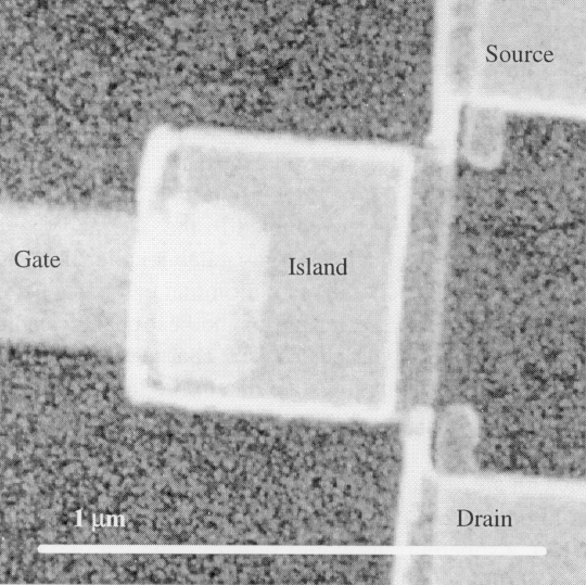
The most widely studied SET device is the capacititvely coupled SET transistor. It consists of a metallic island that is coupled to three electrodes as shown in Fig. 1. Two of the leads are coupled to the island via high resistance tunnel junctions and the third lead (the gate) is capacitively coupled to the island. The transistor shown was fabricated in a Au/SiO/Al three layer process.13 Since aluminum is a superconductor, this device can be operated either in the superconducting state or in the normal state where the superconductivity is suppressed by applying a magnetic field. SET transistors can be made using a wide variety of metals, semiconductors, or conducting polymers.
FIGURE 1 A SEM photo of a capacitively coupled SET transistor. First gold layer was deposited on an oxidized Si substrate and this was patterned by liftoff to form the gate. Next SiO was deposited to electrically isolate the gate and the island. Finally the aluminum source, drain, and island were defined by liftoff. The two tunnel junctions at the corners where the island meets the source and the drain were defined by shadow evaporation. (Courtesy of Erik Visscher)
The electrical characteristics of the capacitively coupled SET transistor
are shown in Fig.2. The current that flows through the two tunnel junctions
can be modulated by changing the charge on the gate. Two current-voltage
curves are shown for this device in the normal state and two curves in
the superconducting state. In the normal state, on the curve labeled q
= 0, no current flows until there is a finite voltage across the two junctions.
This is known as the Coulomb blockade. The origin of the blockade has to
due with the finite energy that is necessary to add an extra electron to
the island. The Coulomb blockade is maximized any time the charge on the
gate is an integer multiple of the charge of an electron, e. The
Coulomb blockade can be suppressed by adjusting gate charge to (n
+ 1/2)e, where n is an integer. When the Coulomb blockade
is suppressed, the curve labeled q = e/2 is observed. In
the superconducting state, hardly any current flows through the device
below a bias voltage of 4![]() /e
even when the Coulomb blockade is suppressed. Here
/e
even when the Coulomb blockade is suppressed. Here ![]() is the superconducting gap.
is the superconducting gap.
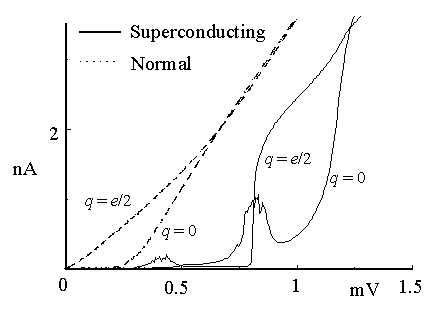
FIGURE 2. The current - voltage characteristics for the same SET transistor in the normal state and in the superconducting state.
A SET transistor can be used to measure charge either in the normal
state or in the superconducting state. Typically, the SET transistor is
voltage biased at a point where there is a large modulation of the current
as a function of the gate charge. The charge that is to be measured is
coupled to the gate and the current through the gate is monitored. By this
means charges much smaller than the charge on an electron can be measured.
The charge resolution that can be achieved is about 10-4 e/
![]() at 10 Hz. SET transistors
offer by far the best charge resolution of any of the available charge
measurement devices. The charge resolution of the SET transistor is better
in the superconducting state due to the larger current modulation at the
optimum bias point.14
at 10 Hz. SET transistors
offer by far the best charge resolution of any of the available charge
measurement devices. The charge resolution of the SET transistor is better
in the superconducting state due to the larger current modulation at the
optimum bias point.14
People familiar with superconducting electronics may be puzzled by the
lack of a supercurrent in Fig. 2. If the tunnel junctions were larger so
that they had a resistance of about 1 ![]() ,
a supercurrent would flow through the two tunnel junctions in series. This
supercurrent would not be sensitive to the charge on the gate. Such large
tunnel junctions exhibit the Josephson effects in the superconducting state
and behave like resistors in the normal state. As the junctions are made
smaller, the resistance of the junctions increases and their capacitances
decrease. The first significant deviation from large junction behavior
occurs when the junction resistance exceeds about 100
,
a supercurrent would flow through the two tunnel junctions in series. This
supercurrent would not be sensitive to the charge on the gate. Such large
tunnel junctions exhibit the Josephson effects in the superconducting state
and behave like resistors in the normal state. As the junctions are made
smaller, the resistance of the junctions increases and their capacitances
decrease. The first significant deviation from large junction behavior
occurs when the junction resistance exceeds about 100 ![]() .
This has to do with the impedance of the environment in which the junction
is embedded. The environment usually consists of the leads which act as
either an antenna or a transmission line and transport high frequency radiation
away from the junction. From the junction's point of view, the environmental
impedance can often be modeled as an ohmic resistor with a value of about
100
.
This has to do with the impedance of the environment in which the junction
is embedded. The environment usually consists of the leads which act as
either an antenna or a transmission line and transport high frequency radiation
away from the junction. From the junction's point of view, the environmental
impedance can often be modeled as an ohmic resistor with a value of about
100 ![]() . (see Fig.
3) The impedance of the environment is in parallel with the junction and
can be neglected if the junction impedance is much lower that the impedance
of the environment. In the large junction limit, the impedance of the junction
is typically 1
. (see Fig.
3) The impedance of the environment is in parallel with the junction and
can be neglected if the junction impedance is much lower that the impedance
of the environment. In the large junction limit, the impedance of the junction
is typically 1 ![]() and
thus the impedance of the environment can be safely neglected. When the
impedance of the junction exceeds about 100
and
thus the impedance of the environment can be safely neglected. When the
impedance of the junction exceeds about 100 ![]() ,
the environment effectively shunts the junction at high frequencies and
it cannot be neglected. This results in additional high frequency damping
which is sometimes reflected in the measured dc characteristics. An excellent
discussion of these effects is given in the second edition of Introduction
to Superconductivity by M. Tinkham.15 For any devices with
impedances larger than 100
,
the environment effectively shunts the junction at high frequencies and
it cannot be neglected. This results in additional high frequency damping
which is sometimes reflected in the measured dc characteristics. An excellent
discussion of these effects is given in the second edition of Introduction
to Superconductivity by M. Tinkham.15 For any devices with
impedances larger than 100 ![]() the
high frequency damping of a low impedance environment should be kept in
mind.
the
high frequency damping of a low impedance environment should be kept in
mind.
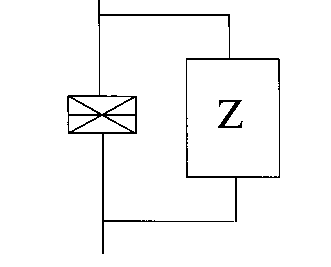
FIGURE 3. A superconducting tunnel junction and the
impedance of the environment it sees at high frequencies. A typical environment
has an impedance of 100 ![]() .
If the junction resistance is much less than 100
.
If the junction resistance is much less than 100 ![]() ,
the effect of the environment can be ignored. For junctions with impedances
larger than 100
,
the effect of the environment can be ignored. For junctions with impedances
larger than 100 ![]() ,
the environment increases the high frequency damping.
,
the environment increases the high frequency damping.
As junctions are made still smaller another qualitative change in the
behavior of the junctions occurs when the resistance of the junctions approaches
the quantum resistance h/e2 = 25 k![]() ,
familiar from the quantum Hall effect. This resistance marks the transition
where the dynamics of a superconducting junction can better be described
by the motion individual electrons and Cooper pairs than by the motion
of individual vortices. Since the voltage across a superconducting junction
is the number of vortices that pass by per second and the current is the
number of electrons that pass by per second, the resistance is the ratio
of the number of vortices that pass by to the number of electrons that
pass by. For resistances much below the quantum resistance many electrons
pass through the junction for every vortex that goes by. In this regime,
the circuit can best be described in terms of the motion of individual
vortices. When the resistance is much higher than the quantum resistance,
many vortices pass through the junction for every electron that passes
by. Here the circuit can best be described in terms of the motion of individual
electrons and Cooper pairs.
,
familiar from the quantum Hall effect. This resistance marks the transition
where the dynamics of a superconducting junction can better be described
by the motion individual electrons and Cooper pairs than by the motion
of individual vortices. Since the voltage across a superconducting junction
is the number of vortices that pass by per second and the current is the
number of electrons that pass by per second, the resistance is the ratio
of the number of vortices that pass by to the number of electrons that
pass by. For resistances much below the quantum resistance many electrons
pass through the junction for every vortex that goes by. In this regime,
the circuit can best be described in terms of the motion of individual
vortices. When the resistance is much higher than the quantum resistance,
many vortices pass through the junction for every electron that passes
by. Here the circuit can best be described in terms of the motion of individual
electrons and Cooper pairs.
When the resistance of the junctions in a circuit is approximately equal
to 25 k![]() , the circuit
must be analyzed quantum mechanically. When this is done for a SET transistor
one finds that the current that flows onto the island and the charge on
the island are noncommuting variables. One consequence of this is that
the supercurrent can be modulated by changing the charge on the gate. It
is possible to use the modulation of the supercurrent to measure the charge
on the gate. Charge measurements can be made more quickly when the supercurrent
is monitored than when the quasiparticle current is monitored because the
output impedance is lower.16 As the resistance is increased
further, the supercurrent is suppressed. For junctions with resistances
more than 100 k
, the circuit
must be analyzed quantum mechanically. When this is done for a SET transistor
one finds that the current that flows onto the island and the charge on
the island are noncommuting variables. One consequence of this is that
the supercurrent can be modulated by changing the charge on the gate. It
is possible to use the modulation of the supercurrent to measure the charge
on the gate. Charge measurements can be made more quickly when the supercurrent
is monitored than when the quasiparticle current is monitored because the
output impedance is lower.16 As the resistance is increased
further, the supercurrent is suppressed. For junctions with resistances
more than 100 k![]() ,
the current that flows is primarily due to quasiparticles and the current-voltage
characteristics has the form shown in Fig. 2.
,
the current that flows is primarily due to quasiparticles and the current-voltage
characteristics has the form shown in Fig. 2.
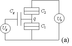
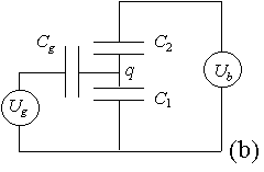
FIGURE 4. If the tunnel junctions resistances are much larger than the quantum resistance then the voltages across the tunnel junctions in circuit (a) can be approximated by solving for the voltages across the equivalent system of capacitors in circuit (b).
For resistances much larger than the quantum resistance it is possible calculate the Coulomb blockade region by first ignoring tunneling and treating the circuit as a system of capacitors (see Fig. 4). When this is done, the voltages across the two junctions can be determined.
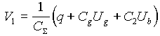
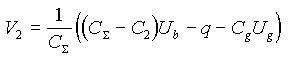
Here q is the charge on the island and ![]() is
the total capacitance,
is
the total capacitance, ![]() =
C1 + C2 + Cg. The
charge on the island can be decomposed into an integer times the charge
of an electron plus an offset charge, q = ne + q0.
The offset charge is due to the polarization of the island by charged defects
in the vicinity of the island. A current will flow through a SET transistor
in the normal state if the voltage across one of the junctions exceeds
e/(2
=
C1 + C2 + Cg. The
charge on the island can be decomposed into an integer times the charge
of an electron plus an offset charge, q = ne + q0.
The offset charge is due to the polarization of the island by charged defects
in the vicinity of the island. A current will flow through a SET transistor
in the normal state if the voltage across one of the junctions exceeds
e/(2![]() ). The
condition that
). The
condition that ![]() and
and
![]() corresponds
to a different diamond shaped region in the Ub - Ug
plane for every value of n. This is shown in the stability diagram
of Fig. 5a.
corresponds
to a different diamond shaped region in the Ub - Ug
plane for every value of n. This is shown in the stability diagram
of Fig. 5a.
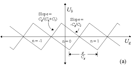
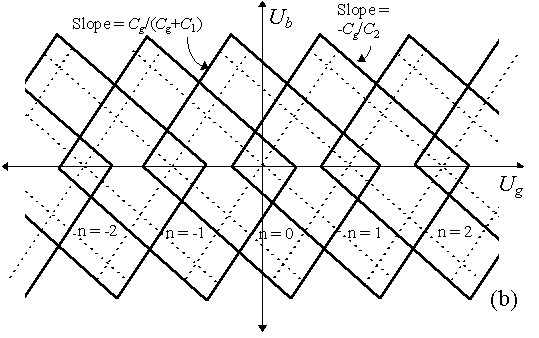
FIGURE 5. (a) The stability diagram for a capacitively coupled SET in the normal state. The Coulomb blockade occurs inside the diamonds. The periodicity along the Ug axes is e/Cg. (b) The stability diagram for the same SET transistor in the superconducting state. In the superconducting state the diamonds overlap. The dotted lines indicate where resonant Cooper pair tunneling can take place. For convenience the offset charge, q0, was taken to be zero in these figures. A nonzero offset charge displaces the stability diagrams along the Ug axis.
The Coulomb blockade occurs inside the diamonds. The periodicity of
the stability diagram is e/Cg along the Ug
axis. In the superconducting state, the condition that no significant quasiparticle
current flow is ![]() and
|
and
|![]() . This results
in the stability diagram shown in Fig. 5b.
. This results
in the stability diagram shown in Fig. 5b.
Measurements of the current through a superconducting SET transistor are shown in Fig. 6. The most prominent feature in the figure is the zigzag pattern across the top which indicates the onset of significant quasiparticle current flow through the SET transistor. This zigzag pattern follows the top of the overlapping diamonds shown in Fig. 5b. The periodicity of the pattern along the gate voltage axis can be used to calculate the gate capacitance and the slopes that form the zigzag pattern can be used to calculate the capacitances of the two junctions using the formulas given in Fig. 5b. The isolated current peaks at a bias voltage of about 0.4 mV are due to the 3e processes described by Maassen van den Brink.17 The intersecting ridges of current are due to the Josephson - quasiparticle cycle.18 Both of these processes involve the tunneling of quasiparticles and Cooper pairs and fall on the dotted lines given in Fig. 5b.
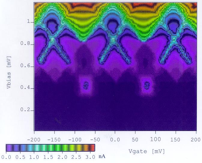
FIGURE 6. Contour plot of the current through a superconducting SET transistor as a function of the bias voltage and the gate voltage.
One of the difficulties with using a capacitively coupled SET transistor is adjusting for the offset charge.19 There are charged defects in the vicinity of the island that act like an extra gate and give the charge on the island a random offset. In circuits consisting of just a small number of SET transistors, one can compensate for the offset charges by coupling a gate to each island. This solution is impractical for circuits consisting of more than a few SET transistors. The effect of the offset charges can be seen in Fig. 7a where the offset charge changed suddenly while a SET transistor was being measured in the normal state. The abrupt change in current at -0.25 mV was caused by a change of the offset charge. It is not uncommon for offset charges to change on the time scale of hours or days. Offset charges can also fluctuate more rapidly. A rapidly fluctuating offset charge is shown in Fig 7b. The existence of fluctuating offset charges makes the behavior of SET transistors somewhat unpredictable. This makes it difficult to design reliable circuits using capacitively coupled SET transistors.
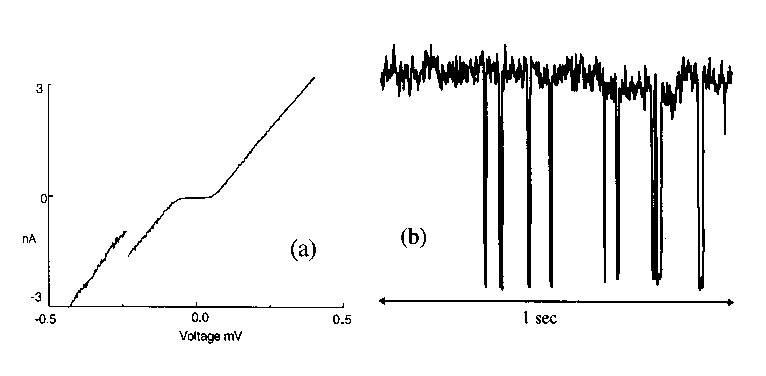
FIGURE 7. (a) The current - voltage characteristic of a capacitively coupled SET transistor in the normal state. At a gate voltage of -0.25 mV the offset charge suddenly changed. (b) The time dependence of the current for a rapidly oscillating offset charge.
Another sort of transistor which is not sensitive to offset charges
is the resistively coupled SET transistor. This also consists of a metallic
island connected to two leads via tunnel junctions but in this case the
control terminal is resistively coupled to the island. To insure that the
charge on the island is well defined, the resistor must have a resistance
greater than the quantum resistance. The stability diagram for a resistively
coupled SET transistor is shown in Fig. 8 for the superconducting state
and the normal state. The region where no significant current flows is
determined again by neglecting tunneling and requiring that the voltages
across the two tunnel junctions satisfy ![]() and
and
![]() in the normal
state and
in the normal
state and ![]() and
and ![]() in the superconducting state. Unlike a capacitively coupled SET transistor,
the characteristics of a resistively coupled SET transistor are not a periodic
function of the gate voltage and are not dependent on the offset charge.
It is therefore easier to design circuits using the resistively coupled
SET transistor.
in the superconducting state. Unlike a capacitively coupled SET transistor,
the characteristics of a resistively coupled SET transistor are not a periodic
function of the gate voltage and are not dependent on the offset charge.
It is therefore easier to design circuits using the resistively coupled
SET transistor.
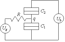
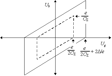
FIGURE 8. The schematic of a resistively coupled SET transistor and its stability diagram. The dashed line in the stability diagram identifies the region where the Coulomb blockade exists in the normal state and the solid line indicates the region where no significant quasi-particle current flows in the superconducting state.
Measurements using SET transistors
Because of their charge sensitivity, SET transistors are very well suited for making precision charge measurements. Many measurements have been made studying charge transport in the SET transistors themselves. By adding electrons to the island of a SET transistor one can investigate the quantum mechanical level spacing in the island, the spin splitting of the quantum mechanical levels in a magnetic field, the interaction of electrons on the island, the coupling of states in the leads to states in the island, the modulation of the shot noise due to the Coulomb blockade, and how electrical transport through the island is coupled to the electromagnetic environment. SET transistors are also very sensitive to applied radiation.20 Photon assisted tunneling has been observed and the absorption of individual photons of microwave radiation can be detected.
SET transistors have been capacitively coupled to a variety of systems
so that the charge motion of those systems could be observed. Metallic
SET transistors have been coupled to semiconductor quantum dots to monitor
the charge fluctuations in the quantum dot.21 They have been
coupled to superconducting particles where it is possible to observe whether
the particle has an odd number or an even number of electrons on it.10
An even number of electrons has a lower energy because all of the electrons
can pair to form Cooper pairs. When the number of electrons is odd one
must remain unpaired which increases the energy by the superconducting
gap ![]() . This odd-even
energy difference can be observed even when the particle contains a billion
electrons. SET transistors have also been scanned over semiconductors to
measure fluctuations in the dopant distribution.22 The spatial
resolution of these measurements was 100 nm and the charge resolution was
0.01 e. Fundamental measurements such as an experiment to make a
more accurate measurement of the fine structure constant have been proposed.23
Furthermore, it is possible to use SET transistors to monitor the occurrence
of unlikely higher order tunnel events which occur at sub zA currents.
. This odd-even
energy difference can be observed even when the particle contains a billion
electrons. SET transistors have also been scanned over semiconductors to
measure fluctuations in the dopant distribution.22 The spatial
resolution of these measurements was 100 nm and the charge resolution was
0.01 e. Fundamental measurements such as an experiment to make a
more accurate measurement of the fine structure constant have been proposed.23
Furthermore, it is possible to use SET transistors to monitor the occurrence
of unlikely higher order tunnel events which occur at sub zA currents.
One of the potential applications of SET devices is a fundamental current standard. In such a device, a known current is established by transferring individual electrons through the device with a frequency f. This results in a current I = ef. A number of different schemes for doing this have been proposed which include modulating the gates coupled to the islands in a series array of tunnel junctions,24,25 modulating the tunnel barriers in a semiconducting quantum dot,26 transferring Cooper pairs in a superconducting circuit,27 and using surface acoustic waves to transport individual electrons.28 The most intensively studied current standard is called an electron pump. It consists of a number of tunnel junctions in series with a gate connected to each island between the junctions. By modulating the gates successively one can draw a single electron through the array of tunnel junctions. The accuracy that has been achieved with this current standard is 15 parts per billion.29 All of the measurements that have been described so far have been made at very low temperatures, typically 0.1 K. This is partly because the SET transistors only work at low temperatures and partly because the phenomena that was being studied with SET transistors only manifest themselves at low temperature. The necessity for very low temperatures is not a great problem for fundamental measurements but it is a problem for applications in general purpose computation which will be discussed in the next section.
SET logic and memories
The small size and low power dissipation of SET circuits makes them potentially useful for the information technology industry. Quite a number of logic schemes have been presented. Some of the schemes are very similar to CMOS where bits are represented by voltage levels.30-33 Figure 9 shows two CMOS-like inverters constructed from SET transistors where the complementary nature of the logic can be seen. Other logic schemes resemble superconducting single flux quantum logic.1 In this case, bits are represented by the presence or the absence of individual electrons. Some logic schemes contain elements that act like electron pumps for moving charge around.34 One scheme is based on the phaselocking of single-electron tunneling oscillations to an ac signal35 and other logic schemes have a neural net architecture.36 Several schemes are based on the bistability of certain element where the electrons can exist in two configurations which have an equivalent energy.37,38 Reversible logic elements39 as well as the more typical irreversible logic schemes have been proposed.
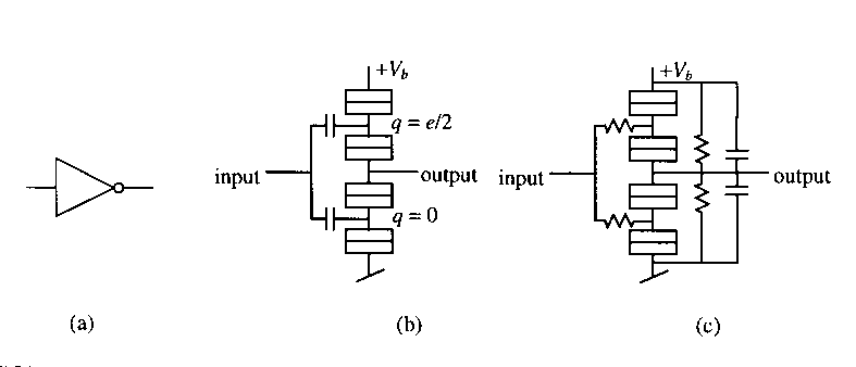
FIGURE 9. (a) The schematic of an inverter. (b) A SET inverter realized with capacitively coupled SET transistors. The offset charges q are specified to insure proper inverter operation. (c) A SET inverter realized with resistively coupled SET transistors.
One practical problem that all of the SET logic schemes face is the necessity for low temperature operation. The problem is that if the energy that is necessary to add an electron to the island of a SET transistor is smaller than the characteristic thermal energy kBT, then the Coulomb blockade will be washed out by thermal fluctuations. The path that must be followed to make circuits that operate at higher temperatures is clear; the dimensions of the devices must be reduced. This will decrease the capacitances and increase the amount of energy that is necessary to add an electron to the island of a SET transistor. In the last few years there has been considerable progress in fabricating smaller devices. A large international effort in nanofabrication is underway that will eventually make molecular-scale devices a reality. It is not yet clear whether the mass production of molecular-scale devices will be economically competitive but it is clear that the devices will become available in the next few years. When SET circuits are scaled down to molecular dimensions, they will function at room temperature. This shrinking of the circuit dimensions has a number of consequences both desirable and undesirable. As the size and the capacitance of the devices decrease, the operating temperature, the operating voltage, and the device packing density increase. These are desirable consequences of the shrinking of SET devices. However, as the dimensions decrease, the electric fields, the current densities, the energy dissipated per switching event, and the power dissipated per unit area all increase. These are undesirable consequences of shrinking.
Another practical problem that many of the logic schemes face is that of offset charges. Most of the logic schemes simply will not work if the offset charges are not somehow eliminated. It is not just the fluctuations of the offset charges that is a problem. Even stationary random offset charges completely disrupt the operation of most logic schemes. The prospects for eliminating the offset charges seem rather dim. It is therefore important to focus on logic schemes which are offset-charge independent.
Exactly how SET devices will contribute to the enterprise of general purpose computation remains unclear. No SET logic scheme is presently threatening to overthrow the semiconductor industry standard CMOS technology. However, different schemes are continuously being proposed and one of these may prove to be superior in some ways to mainstream semiconductor devices. In any case, miniaturization will likely remain an important aspect of dense integrated circuits and single electron effects will almost certainly play a role in devices with very small dimensions.
A separate issue from using SET circuits for logic is the applicability of SET circuits for memories. Right now the memories seem more promising than the logic. Two memories in particular are worth mentioning. The first is an offset-charge independent DRAM cell which was described by Likharev and Korotkov.40 In their circuit, a bit is represented by the presence or absence of a charge of a few electrons which is stored on an island. The charge on the island is monitored by a SET transistor. When the memory cell is read, the circuit is biased so that any charge on that may be on the island is removed. If there was charge on the island when the memory cell is read, the current through the SET transistor undergoes oscillations as each electron tunnels off the island. If there was no charge stored on the island there are no oscillations of the current. The oscillations of the current through the SET transistor occur for any value of the offset charge.
Another type memory called a single-electron MOS memory (SEMM) is also based on the motion of individual electrons.41,42 This device is very similar to a conventional floating gate MOS memory. The charge on a floating gate modulates the conduction through a channel nearby the gate. The gate is made so small that even if one electron is added to the floating gate, the conduction through the channel changes appreciably.
Conclusions
Single-electron tunneling devices are contributing to our understanding of how charge is transported in tunnel junction circuits and how to treat circuits quantum mechanically. It is likely that SET circuits will make a lasting impact in the field of precision measurements either as a fundamental standard of capacitance, or a fundamental current standard, or both. A great number of SET logic schemes are being proposed but it is not yet clear if any of them will be competitive with semiconductor circuits. SET memories that should work at very high packing densities have been proposed. The realization of these memories will have to wait for fabrication technologies that can produce them at those densities.
Acknowledgments
Support from Esprit project 22953, CHARGE, is gratefully acknowledged.
References
1. D.V. Averin and K. K. Likharev, ''Single-electronics: A correlated
transfer of single electrons and Cooper pairs in systems of small tunnel
junctions,'' in Mesoscopic Phenomena in Solids, eds. B.L. Altshuler, P.
A. Lee, and R. A. Webb, Elsevier (1991).
2. M. H. Devoret, D. Esteve, and C. Urbina, ''Single Electron transfer
in metallic nanostructures,'' Nature 360 p. 547 (1992). 3. H. Grabert and
M. H. Devoret, Eds., Single Charge Tunneling, Plenum Press, London (1991).
4. K. K. Likharev,
''Physics and possible applications of single-electron devices,'' FED Journal
6 p. 5 (1995).
5. M. I. Lutwyche, and Y. Wada, ''Estimate of the ultimate performance
of the single-electron transistor,'' J. Appl. Phys. 75 p. 3654 (1994).
6. A T. Johnson, L. P. Kouwenhoven, W. de Jong, N. C. van der Vaart, and
C. J. P. M. Harmans, ''Zero-dimensional states and single electron charging
in quantum dots,'' Physical Review Letters 69 p. 1592 (1992).
7. D. C. Ralph, C. T. Black, and M. Tinkham, ''Spectroscopy measurements
of discrete electronic states in single metal particles, ''Phys. Rev. Lett.
74 3241 (1995).
8. S. Tarucha, D. G. Austing, T. Honda, R. J. van der Hage, and L. P. Kouwenhoven,
''Shell filling and spin effects in a few electron quantum dot,'' PRL 77
p. 3613 (1996).
9. N. C. van der Vaart, A. T. Johnson, L. P. Kouwenhoven, D. J. Maas, W.
de Jong, M. P. de Ruyter van Steveninck, A. van der Enden, and C. J. P.
M. Harmans, ''Charging effects in quantum dots at high magnetic field,''
Physica B189 p. 99 (1993).
10. C. T. Black, D. C. Ralph, and M. Tinkham, ''Spectroscopy of the superconducting
gap in individual nanometer-scale aluminum particles, '' Phys. Rev. Lett.
76 688 (1996).
11. H. Birk, M.J.M. de Jong, and C. Schnenberger, ''Shot noise suppression
in the single-electron tunneling regime,'' Phys. Rev. Lett. 75 p. 1610
(1995).
12. G. -L. Ingold, P. Wyrowski, and H. Grabert, ''Effect of the electromagnetic
environment on the single electron transistor, '' Zeitschrift für
Physik 85 p. 443 (1991).
13. E. H. Visscher, S. M. Verbrugh, J. Lindeman, P. Hadley, and J. E. Mooij,
"Fabrication of multilayer single-electron tunneling devices,"
Applied Physics Letters 66 p. 305 (1995).
14. A. N. Korotkov, "Charge sensitivity of superconducting single-electron
transistor," Appl. Phys. Lett. 69, p. 2593 (1996).
15. M. Tinkham, Introduction to Superconductivity, McGraw-Hill (1996).
16. A. B. Zorin, ''Quantum-limited electrometer based on single Cooper
pair tunneling,'' PRL 76 p. 4408 (1996).
17. A. Maassen van den Brink, A. A. Odintsov, P. A. Bobbert, G. Schön,
''Coherent Cooper pair tunneling in systems of Josephson junctions: effects
of quasiparticle tunneling and of the electromagnetic environment,'' Zeitschrift
für Physik 85 p. 459 (1991).
18. T. A. Fulton, P.L. Gammel, D. J. Bishop, L. N. Dunkleburger, and G.
J. Dolan, "Observation of combined Josephson and charging effects
in small tunnel junction circuits," Phys. Rev. Lett. 63 p. 1307 (1989).
19. A.B. Zorin, F.-J. Ahlers, J. Niemeyer, T. Weimann, H. Wolf, V.A. Krupenin,
and S.V. Lotkhov, "Background charge noise in metallic single-electron
tunneling devices," Physical Review B 53, p. 13682 (1996).
20. J. M. Hergenrother, J. G. Lu, M. T. Touminen, D. C. Ralph, and M. Tinkham,
Phys. Rev. B 51, p. 9407 (1995).
21. D. Berman, N.B. Zhitenev, R.C. Ashoori, H.I. Smith and M.R. Melloch,
"The Single-Electron Transistor as a Charge Sensor for Semiconductor
Applications," to be published in the Journal of Vaccuum Science and
Technology B.
22 M. J. Yoo, T. A. Fulton, H. F. Hess, R. L. Willett, L. N. Dunkleberger,
R. J. Chichester, L. N. Pfeiffer, K. W. West, "Scanning single-electron
transistor microscopy: Imaging individual charges," Science 276 p.
579 (1997).
23. Alan F. Clark,
Neil M. Zimmerman, Edwin R. Williams, A. Amar, Dian Song, F. C. Wellstood,
C. J. Lobb , and R. J. Soulen, Jr., "Application of Single Electron
Tunneling: Precision Capacitance Ratio Measurements'', Appl. Phys. Lett.
66, 2588 (1995).
24. L. J. Geerligs, V.F Anderegg, P.A.M. Holweg, J. E. Mooij, H. Pothier,
D. Esteve, C. Urbina, and M. H. Devoret, ''Frequency locked turnstile device
for single electrons, ''Phys. Rev. Lett. 64 p. 2691(1990).
25. H. Pothier, P. Lafarge, C. Urbina, D. Esteve, and M. H. Devoret, ''Single
electron pump based on charging effects, ''Europhys. Lett. 17 p. 249 (1992).
26. L. P. Kouwenhoven, A. T. Johnson, N. C. van der Vaart, and C. J. P.
M. Harmans, ''Quantized current in a quantum dot turnstile using oscillating
tunnel barriers,'' Physical Review Letters 67 p. 1626 (1991).
27. L.J. Geerligs, S.M. Verbrugh, P. Hadley, J.E. Mooij, H. Pothier, P.
Lafarge, C. Urbina, D. Esteve, and M.H Devoret, "Single Cooper pair
pump," Zeitschrift für Physik B 85 p. 349-355 (1991).
28. V. I. Talyanskii, J. M. Shilton, M. Pepper, E. H. Linfield, D. A. Ritchie,
and C.J.B. Ford, ''Single electron transport in one-dimensional channel
by high-frequency surface acoustic waves, '' Proceedings of the Workshop
on Fundamental aspects of applications of single electron devices, p. 19
(1997).
29. Mark W. Keller, John M. Martinis, Neil M. Zimmerman, and Andrew H.
Steinbach, "Accuracy of Electron Counting Using a 7-Junction Electron
Pump'', Appl. Phys. Lett. 69, 1804 (1996).
30. Tucker, J. R., "Complementary digital logic based on the Coulomb
blockade," J. Appl. Phys. 72 p. 4399 (1992).
31. Nobuyuki Yoshikawa, Yasuyuki Jinguu, Hiroshi Ishibashi, and Masanori
Sugahara, "Complementary digital logic using resistively coupled single-electron
transistor," Jpn J. Appl. Phys. 35, p. 1140 (1996).
32. R. H. Chen,
A. N. Korotkov, and K. K. Likharev, ''Single-electron transistor logic,''
Appl. Phys. Lett. 68 p. 1954 (1996).
33. A. N. Korotkov,
R. H. Chen, and L. K. Likharev, ''Possible performance of capacitively
coupled single-electron transistors in digital circuits,'' J. Appl. Phys.
78, p. 2520 (1995).
34. M.G. Ancona, ''Design of computationally useful single-electron digital
circuits,'' J. Appl. Phys. 79, p. 526 (1996).
35. T. Ohshima, and R.A. Kiehl, "Operation of bistable phase-locked
single-electron tunneling logic elements," J. Appl. Phys 80 p. 912
(1996).
36. M.J. Goossens, J. H. Ritskes, C.J.M. Verhoeven, and A.H.M. van Roermun,d
"Neural networks with periodic single-electron tunneling transistors,"
Proceedings of the 1997 European Conference on Circuit Theory and Design
(ECCTD'97) pp. 937-941 (1997).
37. A. N. Korotkov,
''Wireless single-electron logic biased by alternating electric field,''
Appl. Phys. Lett. 67 p. 2412 (1995).
38. P. D. Tougauw and C. S. Lent, ''Logical devices implemented using
quantum cellular automata,'' J. Appl. Phys. 75 p. 1818 (1994).
39. K. K. Likharev,
and A. N. Korotkov, ''Single-Electron Parametron: Reversible Computation
in a Discrete State System,'' Science 273, p. 763 (1996).
40. Likharev, K.
K., and A. N. Korotkov, "Ultradense hybrid SET/FET dynamic RAM: Feasibility
of background-charge-independent room-temperature single-electron digital
circuits," Proceedings of ISDRS'95 (1995).
41. K. Yano, T. Ishii, T. Kobayashi, F. Murai, and K. Seki, ''Room-temperature
single-electron memory,'' IEEE Transactions on Electron Devices 41, p.
1628, (1994).
42. Lingjie Guo, Effendi Leobandung, and Stephen Y. Chou, ''A silicon single-electron
transistor memory operating at room temperature,'' Science 275, p. 649
(1997).