| APPLIED PHYSICS LETTERS | VOLUME 74, NUMBER 7 | 15 FEBRUARY 1999 |
Single-electron tunneling devices offer a means to manipulate individual electrons. Their advantages of small size and low power dissipation have stimulated a number of proposals for their use in some future generation of computation technology, [1] yet relatively few such circuits have been measured. Many techniques exist for creating single-electron devices, including the use of scanning probes to manipulate the nanometer scale structures necessary for room temperature operation. These structures have so far been limited to planar layouts, which severely restrict possible circuit architectures because voltage gain becomes difficult to achieve and wire crossing is impossible. The most widely used fabrication technique, electron beam lithography, allows one to build multilayered circuits that can circumvent these problems. E-beam lithography, however, has a minimum resolution of ~ 10 nm; consequently, single-electron effects can usually only be observed at low temperature ( < 1 K) in devices built this way. Up to now, technologically oriented research has primarily focused on the further miniaturization of basic components, while ignoring the fabrication and testing of more complex circuits. We feel it is worthwhile to consider low-temperature prototypes of these circuits to estimate the usefulness of their future high-temperature counterparts.
In this Letter we report on a multilayer circuit consisting of two strongly coupled Al/AlxOy islands fabricated using electron beam lithography and measured at low temperature. The circuit demonstrates negative differential resistance (NDR) due to the tunneling of a single electron into one of the islands. Device applications of NDR--including amplification, logic and memory--have been extensively discussed in literature regarding resonant tunnel diodes. [2] Single-electron NDR has heretofore been predicted in systems of multiple islands, where electrostatic repulsion between electrons in different islands regulates the source-drain current. [3,4] Our circuit offers the advantage of requiring only two islands, rather than six arranged in a zig-zag, [3] or four in a ring geometry. [4]
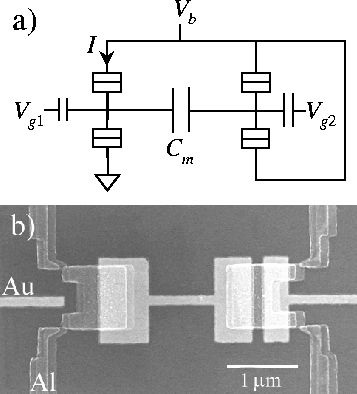
The equivalent circuit diagram of our device is shown in Fig. 1a. The left island forms a single-electron transistor (SET), allowing a current I to flow between the voltage source Vb and ground. The right island, however, merely traps charge entering from the source, and so acts as an ''electron box.''[5] The two islands are also coupled by a large mutual capacitance Cm, but electron tunneling between the islands is forbidden. Additional control is provided by tuning gate voltages Vg1 and Vg2, which determine the electrostatic potentials and charge states of the islands. The current through a solitary SET depends both upon the bias voltage across its terminals and the gate voltage. In our setup the SET feels an additional effective gate voltage due to the charge state of the electron box. Whenever a single extra electron tunnels into the box, there is a discontinuous change in charge on Cm, resulting in a jump in the effective gate voltage felt by the SET and consequently a jump in the current.
Figure 1b shows an SEM photograph of our device, consisting of an Al island layer (medium gray) and an underlying Au gate layer (light gray), with a thin intermediate SiO layer providing electrical insulation. The tunnel junctions are formed at the corners of the islands where they meet the pointed ends of the leads. Three sections of the gate layer are visible; the two structures extending from the left and right sides are the tuning gates, while the central dumbbell-shaped structure underlapping both islands forms the mutual capacitor Cm.
The device was fabricated on a silicon substrate with a 250 nm thermally oxidized top layer, and patterned using standard electron beam lithography with a high resolution pattern generator in a double layer PMMA resist. The bottom gate layer was formed by evaporating 5 nm of Ti and 20 nm of Au perpendicular to the substrate surface. Directly after lift-off the whole sample was covered with a 32 nm insulating SiO layer. To ensure good step coverage, SiO was evaporated under four perpendicular angles oriented 30o to the substrate surface normal. The islands, leads and contact pads were written in a new bilayer of PMMA after aligning the electron beam pattern generator to Au markers defined in the gate layer. A pattern generator alignment resolution of 50 nm or less is necessary to produce good results. The tunnel junctions were formed using the standard technique of double angle shadow evaporation of Al through the resist mask, oxidizing the Al between evaporations.[8] Contact pads were coupled to the gates by 0.2 pF overlap capacitors. To protect the junctions from high voltage static discharges, the leads were shunted on-chip by 12 pF overlap capacitors.
The device was measured in a standard 3He-4He
dilution refrigerator at a base temperature of 4 mK (electron temperature
~ 27 mK). An external magnetic field of 1 T was applied to suppress superconductivity.
From high-bias measurements, the total tunneling resistances of the SET
and the box were determined to be 7 MW and 13
MW, respectively. Having verified that all the
junctions had finite tunneling resistances, the leads were connected as
in Fig. 1a. No leakage current through the SiO insulating layer was detected.
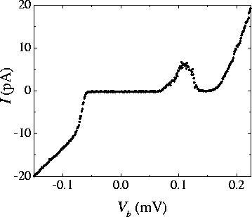
A typical measurement of the current I as a function of source-drain bias Vb is plotted in Fig. 2. The device clearly demonstrates NDR in the bias range of 110-130 mV, with a peak-to-valley ratio in excess of 30. A more precise determination of this ratio is difficult, however, due to an enhancement of low-frequency noise around the NDR onset, possibly caused by thermally activated charge fluctuations in the box. Fig. 2 also shows enhanced differential conductance at Vb = -70 mV. This feature is due to a mechanism similar to NDR, but where the trapping of an extra electron in the box suddenly pulls the SET out of Coulomb blockade.
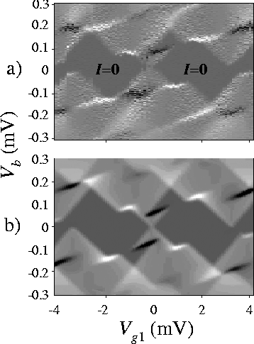
The NDR features can be shifted by tuning the gate voltages. The dependence on Vg1 is shown in Fig. 3a, where the differential conductance dI/dV is plotted in gray-scale as a function of Vb and Vg1. Here we see diamond-shaped Coulomb blockaded regions (marked by ''I = 0''), fractured by the discrete charging of the box. Black regions represent NDR, while white represents enhanced differential conductance.
The electrostatic potentials of a two-island circuit may be expressed analytically in terms of the applied voltages, the charge state of each island, and the capacitances. [9] Consequently, the slopes of the various thresholds in Fig. 3a, combined with similar measurements (such as by sweeping Vg2), allow us to fully characterize the capacitor network of the device. The junction capacitances were all approximately 0.3 fF, while Cm was estimated to be 0.64 fF. Using our estimated capacitances, we have carried out simulations of the device using a master equation approach combined with the orthodox theory of single-electron tunneling. [10,11] The simulation of Fig. 3b shows dI/dV as a function of Vb and Vg1, assuming a temperature of 25 mK. It correctly reproduces the position and character of the features in Fig. 3a, with only minor variations. We similarly found excellent agreement between experiment and simulation when Vg2 was swept.
Simulations show that the magnitude of NDR gradually decreases with increasing temperature, vanishing when:
| (1) |
Here C1(2) is the total capacitance of the SET (box) including the coupling capacitance Cm. This maximum temperature was approximately 150 mK for our device, and measurements at T=100 mK confirmed that NDR exists, but is greatly diminished, at this higher temperature. Simulations also predict that, for sufficiently large Cm>3Cj, multiple NDR regimes should appear. We estimate that a fully optimized device using our multilevel technique could yield a Cm/Cj ratio of 10, making possible the study of very strongly coupled metallic islands.
In conclusion, we have measured negative differential resistance due to single-electron switching in a circuit with a strong capacitive coupling between two islands. Measurements were in excellent quantitative agreement with semiclassical simulations. Our multilevel fabrication process allows inter-island couplings unmatched by any planar architecture, perhaps allowing the observation of new physical effects. Preliminary measurements have produced encouraging results, and more research in this regime is forthcoming. Our measurements also demonstrate the strong influence that the introduction of a single electron can have on the conductance of a small island of charge--an effect that will only gain importance as the present trend of transistor miniaturization proceeds apace.