SET logic
P. Hadley
Department of Applied Physics and DIMES, Delft University of Technology, PO Box 5046, 2600 GA Delft, The Netherlands
Abstract. Single-electron tunneling transistors can manipulate individual electrons. These device dissipate little power and can be fabricated in sizes ranging down to a molecular scale. It has been suggested that large scale integration of single-electron transistors could result in logic circuits with a high device packing density. Recently a number of different logic schemes using single-electron tunneling transistors have been proposed. A brief overview of these developments will be presented here.
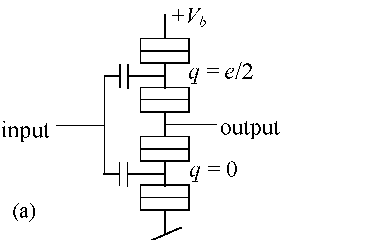
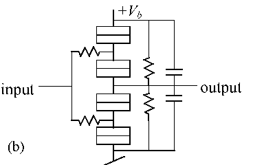
Single-electron tunneling (SET) devices can monitor and manipulate the motion of individual electrons.1-3 The small size and low power dissipation of SET circuits makes them potentially useful for the information technology industry. In the first SET logic scheme proposed by Likharev and Averin, bits were represented by individual electrons.1 This logic (called single-electron logic) has an architecture similar to superconducting single flux quantum logic where individual magnetic flux quanta are manipulated.4 Ancona also proposed a logic scheme where bits were represented by individual electrons but he proposed building circuits with a regular cellular structure with local connections as in a cellular automata.5 Tucker6 and Yoshikawa7 et al. suggested the use of single-electron tunneling transistors in an architecture very similar to CMOS. In this case the bits are represented by voltage levels.8,9 Figure 1 shows two CMOS-like inverters constructed from SET transistors. Tougaw and Lent suggested that the electron configuration in a cluster of quantum dots could be used to encode the information.10 The clusters of quantum dots are placed very close together but they are not electrically connected. The information passes from one cluster to the next via the Coulomb interaction between the electrons. Computation proceeds locally as in a cellular automata architecture. Korotkov proposed a similar computational scheme using clusters not connected by wires.11 Unlike Tougaw and Lent, Korotkov suggested the use of an ac driving field so that the energy needed to drive the computation could be coupled into each of the clusters directly. Ohshima and Kiehl also proposed a SET logic scheme using an ac pump (tunneling phase logic).12 In this scheme the information is not coded in the configuration of some charge on a cluster but it is coded in the relative phase between the ac pump and the periodic single-electron tunneling oscillations. Likharev and Korotkov also proposed reversible logic elements13 where the amount of energy dissipate per switching event could be much less than kBT. There have also been several suggestions to use single-electron tunneling transistors to build neural nets. Goossens et al. suggested exploiting the periodic transfer characteristics of a SET transistor to build neural nets14 while the quantum neuromorphic networks of Bandyopadhyay et al.15 function more like a traditional Hopfield machine.
FIGURE 1. (a) A SET inverter realized with capacitively coupled SET transistors. The offset charges q are specified to insure proper inverter operation. (b) A SET inverter realized with resistively coupled SET transistors.
Although many logic schemes have been proposed, no logic family has been thoroughly characterized experimentally. One of the problems is that it has been difficult to fabricate complex circuits with the very small feature sizes necessary (< 100 nm) for single electronics circuits. In order for SET circuits to function, the energy that is necessary to add an electron to a device must be larger than the characteristic thermal energy kBT. If this is not the case, then the single-electron effects will be washed out by thermal fluctuations. In order to make the electron addition energy (also called the charging energy) large, the capacitance of the devices must be made so small that e2/C is much larger than kBT, where C is the capacitance of the device. This requires that the dimensions of the devices be very small. Presently, complex SET circuits are made with critical dimensions of about 50 nm.16 At this scale the circuits are still not very reliable and only work at low temperature. There are many reports of individual SET transistors that work at room temperature but those fabrication technologies do not allow wires to cross and no room temperature transistors with voltage gain have been produced. These two conditions are necessary for making complex logic circuits. Recently there has been considerable progress in fabricating smaller devices. It is likely that complex molecular-scale devices will be fabricated reasonably soon. When that happens SET circuits will operate at room temperatures.
Another problem that SET circuits face is the presence of offset charges.17 Offset charges are charged defects in or near SET circuits. They can be interstitial atoms or charged vacancies which can polarize a SET transistor with a charge that is a fraction of an electron. SET circuits are extremely sensitive to charge; the operation of many circuits is completely disrupted by the presence of the offset charges. Most of the logic schemes described above simply will not work if the offset charges are not somehow eliminated. The prospects for eliminating the offset charges seem rather small. It is therefore important to focus on logic schemes such as the resistively coupled SET transistor logic of Yoshikawa et al.7 which is offset-charge independent.
The future role that SET devices will have in general purpose computation remains unclear. The large scale realization of SET circuits that function at room temperature will have to wait for advances in fabrication technology that will allow for the mass production of molecular scale devices. No SET logic scheme is presently threatening to overthrow the semiconductor industry standard CMOS technology. However, different schemes are continuously being proposed and one of these may prove to be superior in some ways to mainstream semiconductor devices. In any case, miniaturization will likely remain an important aspect of dense integrated circuits and single electron effects will almost certainly play a role in devices with very small dimensions.
Acknowledgments
Support from Esprit project 22953, CHARGE, is gratefully acknowledged.
References
1. D.V. Averin and K. K. Likharev, ''Single-electronics: A correlated
transfer of single electrons and Cooper pairs in systems of small tunnel
junctions,'' in Mesoscopic Phenomena in Solids, eds. B.L. Altshuler, P.
A. Lee, and R. A. Webb, Elsevier (1991).
2. K. K. Likharev,
''Physics and possible applications of single-electron devices,'' FED Journal
6 p. 5 (1995).
3. M. I. Lutwyche, and Y. Wada, ''Estimate of the ultimate performance
of the single-electron transistor,'' J. Appl. Phys. 75 p. 3654 (1994).
4. K.K.
Likharev, "Rapid single flux quantum logic."
5. M.G. Ancona, ''Design of computationally useful single-electron
digital circuits,'' J. Appl. Phys. 79, p. 526 (1996); M.G. Ancona, ''Systolic
processor designs using single-electron digital circuits,'' Superlattices
and Microstructures 20 (1996).
6. Tucker, J. R., "Complementary digital logic based on the Coulomb
blockade," J. Appl. Phys. 72 p. 4399 (1992).
7. Nobuyuki Yoshikawa, Yasuyuki Jinguu, Hiroshi Ishibashi, and Masanori
Sugahara, "Complementary digital logic using resistively coupled single-electron
transistor," Jpn J. Appl. Phys. 35, p. 1140 (1996).
8. R. H. Chen, A.
N. Korotkov, and K. K. Likharev, ''Single-electron transistor logic,''
Appl. Phys. Lett. 68 p. 1954 (1996). 9. A.
N. Korotkov, R. H. Chen, and L. K. Likharev, ''Possible performance of
capacitively coupled single-electron transistors in digital circuits,''
J. Appl. Phys. 78, p. 2520 (1995).
10. P. D. Tougauw and C. S. Lent, ''Logical devices implemented using quantum
cellular automata,'' J. Appl. Phys. 75 p. 1818 (1994).
11. A. N. Korotkov,
''Wireless single-electron logic biased by alternating electric field,''
Appl. Phys. Lett. 67 p. 2412 (1995). 12. T. Ohshima, and R.A. Kiehl,
"Operation of bistable phase-locked single-electron tunneling logic
elements," J. Appl. Phys 80 p. 912 (1996).
13. K. K. Likharev,
and A. N. Korotkov, ''Single-Electron Parametron: Reversible Computation
in a Discrete State System,'' Science 273, p. 763 (1996).
14. M.J. Goossens, J.H. Ritskes, C.J.M. Verhoeven, and A.H.M. van Roermund,
"Neural networks with periodic single-electron tunneling transistors,"
Proceedings of the 1997 European Conference on Circuit Theory and Design
(ECCTD'97), p 937-941 (1997).
15. S. Bandyopadhyay, V.P. Roychowdhury, and X. Wang, "Computing with
Quantum Dots: Novel architectures for nanoelectronics," Phys. Low-Dim.
Struct., 8/9 pp. 29-82 (1995).
16. E. H. Visscher, S. M. Verbrugh, J. Lindeman, P. Hadley, and J. E. Mooij,
"Fabrication of multilayer single-electron tunneling devices,"
Applied Physics Letters 66 p. 305 (1995).
17. A.B. Zorin, F.-J. Ahlers, J. Niemeyer, T. Weimann, H. Wolf, V.A. Krupenin,
and S.V. Lotkhov, "Background charge noise in metallic single-electron
tunneling devices," Physical Review B 53, p. 13682 (1996).