Single-Electron Effects in Metals and Nanotubes for Nanoscale Circuits
Peter Hadley, Pieter Heij, Günther Lientschnig, Tijs Teepen, Henk Postma, and Cees Dekker, Department of Applied Sciences and DIMES, Delft University of Technology, The Netherlands.
Abstract
As circuits are made smaller, certain new physical phenomena will appear. When the capacitance of components becomes so small that adding a single electron to that component causes the voltage to jump significantly, then single-electron effects will have to be included in the device models. This can have important consequences for the conductance through the device and the noise that is observed. Transistors based on single-electron effects have been made using metal tunnel junctions, silicon technology and conducting polymers. Here the status of single-electronic circuits made from metal tunnel junctions and carbon nanotubes is discussed.
Kurzfassung
Wenn die integrierten Schaltkreise sehr klein werden, können bestimmte neue physikalische Effekte auftreten. Falls die Bauelemente eine so geringe Kapazität aufweisen, dass das Hinzufügen eines einzigen Elektrons mit einer signifikanten Spannungsänderung einhergeht, müssen Einzelelektronen-Effekte in der Modellierung dieser Komponenten berücksichtigt werden. Diese Effekte können weitreichende Konsequenzen auf die Leitfähigkeit durch das Bauelement und auf das beobachtete Rauschen haben. Auf Einzelelektronen-Effekten basierende Transistoren wurden mithilfe von Metall-Tunnelkontakten, mit Siliziumtechnologie und mit leitenden Polymeren hergestellt. Der gegenwärtige Stand von Einzelelektronen Bauelementen, die mit Metall-Tunnelkontakten und mit Kohlenstoff-Nanoröhrchen realisiert wurden, wird in diesem Artikel erörtert.
1 Introduction
Single-electron tunneling devices can manipulate individual electrons. Because a minimum of charge is transported in these circuits, they do not dissipate much power. This has stimulated considerable discussion about how single-electron devices could be used in dense integrated circuits. A variety of single-electron logic schemes have been put forward but relatively few logic elements have been tested experimentally. A good overview of single-electron circuits can be found in a recent review by Likharev [1].
2 Metal tunnel junction SET's
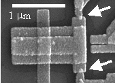
The basic building block of most single-electron circuits is the single-electron transistor (SET). A scanning electron microscope image of a single-electron transistor is shown in Fig. 1. In the transistor, a metal island is connected to source and drain leads by small tunnel junctions. The tunnel junctions are the small points in the figure where the source and drain leads make contact with the island. The island is also coupled capacitively to two gates. The gate on the left is an overlap gate (like a parallel plate capacitor) and the gate on the right is a planar gate. When a bias voltage is placed across the source and drain leads, a current can flow due to sequential tunneling of electrons from the source onto the island and then from the island to the drain. Each time the number of electrons on the island changes by one electron charge e, the voltage on the island changes by e/C S. Here C S is the total capacitance of the island. For small bias voltages, the energy required to add an electron to the island can be greater than the energy provided by the bias voltage. In this case, no electrons tunnel onto the island and no current flows. This is called the Coulomb blockade. Figure 2 shows the conductance of a single-electron transistor as a function of the bias voltage and the gate voltage. The diamond-shaped regions at zero bias voltage are regions of Coulomb blockade. The figure shows that the current through a SET transistor is a periodic function of the gate voltage.
Fig. 1 A scanning electron microscope image of a single-electron transistor. The white arrows point to the two tunnel junctions. The source and drain leads are at the top and the bottom of the image. The vertical line to the left of the tunnel junctions is an overlap gate that couples capacitively to the island. To the right of the tunnel junctions is a planar gate.
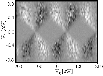
Fig. 2 The conductance of a single-electron transistor (dI/dVg) is plotted versus the bias voltage and the gate voltage. The gray diamonds are regions of Coulomb blockade (zero conduction). White is positive differential conductance and black is negative differential conductance.
A single-electron transistor switches from the off-state (Coulomb blockade) to the on-state (conducting) when half an electron is added to the gate. This is orders of magnitude less charge than is necessary at the gate of a field-effect transistor to switch it from off to on. Single-electron transistors are the most sensitive charge sensing devices available. They can detect smaller amounts of charge than a field-effect transistor and they can detect a larger amount of charge faster than a field effect transistor. It is therefore in applications where charge sensitivity is required that single-electron transistors excel.
The measurements in Fig. 2 were performed at a temperature of 50 mK. The low temperature was necessary to ensure that thermal fluctuations, with a typical energy of kBT, do not provide the energy necessary to add electrons to the island. The energy necessary to add an electron to the island is called the charging energy EC = e2/2C S. For a single-electron transistor to function properly, the thermal fluctuations must be much smaller than the charging energy. This can be achieved by making the total capacitance of the island very small.
Room temperature operation of single-electron transistors based on metal tunnel junctions was reported by Pashkin et al. [2] They fabricated transistors with aluminum islands with diameters down to 2 nm using electron-beam lithography. These transistors had a total capacitance of about 1 aF and a charging energy of about 100 meV.
3 Carbon nanotube SET's
Carbon nanotubes are molecules consisting exclusively of carbon that have a cylindrical form of a few nanometers in diameter and a few microns in length. The tubes can either be semiconducting or metallic, the conductivity depending on their diameter and their molecular structure. Diodes, field-effect transistors, and single-electron transistors have been made from carbon nanotubes. Tans et al. made a field-effect transistor by laying a semiconducting nanotube between two platinum electrodes. [3] The conductance through the nanotube was modulated by a backgate. Yao et al. observed diode-like behavior in a nanotube kink. [4] At the kink, a metallic tube and a semiconducting tube fuse together to create an intramolecular metal-semiconductor junction that is only a few atoms in cross-section. The metal-semiconductor kink junction behaves like a molecular diode. A single-electron transistor has been made by placing a metallic nanotube between two metal electrodes. [5] In this case, the nanotube is the island of the SET and the contact resistances at the electrodes form the tunnel junctions of the transistor. This sort of SET has to be measured at low temperature because the charging energy is smaller than room temperature thermal fluctuations. Room temperature operation of nanotube SET's has been achieved by making two buckles in a metallic nanotube. Postma et al. used the tip of an atomic force microscope to put buckles in a carbon nanotube. [6] The tube buckles much the same way as a drinking straw buckles when it is bent too far. The buckles act as tunnel barriers to electron transport and isolated a 25 nm section of the nanotube that acted as the island of a single-electron transistor. The total capacitance achievable in this case is about 1 aF. In what may be the ultimate size reduction for carbon nanotube electronics, Park et al. placed a C60 molecule between electrodes spaced 1.4 nm apart. [7] The total capacitance of the C60 molecule in this configuration was about 0.3 aF.
The smallest capacitances that have been achieved in metallic junction SET's and carbon nanotube SET's are about the same, ~ 1 aF. This is perhaps not so surprising because the physics of the operation is the same in both cases; it is just the materials that have been changed.
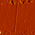
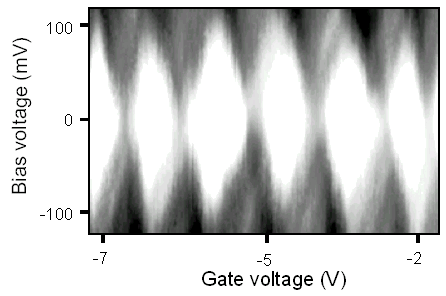
Fig. 3 The top picture is an atomic force microscope image of a nanotube that is lying between platinum electrodes spaced 500 nm apart. The lower part of the figure is the conductance, |dI/dVb|, of a nanotube buckle SET. The charging energy in this case was 100 meV and the measurement was taken at 77 K. White is zero conductance in this image. The white diamonds are regions of Coulomb blockade.
Apart from diodes and transistors, it has also been suggested that carbon nanotubes could be used as interconnects in integrated circuits. Nanotubes are remarkably good electrical conductors and have a resistance similar to the resistance copper wires would have if they were made 1 nm in diameter. However, copper wires can be made in many shapes. Long wires can be made wider and thicker to reduce the resistance of long interconnects. [8] This flexibility gives copper an advantage in integrated circuits where many interconnect layers are needed.
4 Gain
Figure 4 shows the voltage gain of a selection of transistors as a function of feature size. The feature size is defined as the distance from the source contact to the drain contact. There is a dashed line at a voltage gain of 1. To achieve a voltage gain greater than one in a single-electron transistor, the gate capacitance must be larger than the tunnel junction capacitance. This is most effectively achieved by making overlap gate capacitors. Planar gates typically have too low capacitance for the voltage gain criterion. In most published reports of single-electron transistors, the voltage gain is less than one. Figure 4 shows that there is a general trend towards lower gain for smaller devices. This is also true for CMOS. The dotted line is a rough indication of the gain that is achievable for CMOS transistor. Pikus et al. calculated that CMOS transistors will no longer exhibit voltage gain for a gate length less than 10 nm. [9] Any technology that aspires to replace CMOS should have a signal gain greater than one for a feature size less than 10 nm. There are presently no nanodevices that meet this criterion.
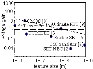
Fig. 4 The voltage gain is plotted against the feature size for various devices. The overall trend is that the voltage gain decreases at the size decreases. The numbers indicate the reference for each data point.
5 Output impedance
The speed of a circuit is related to the output impedance of devices in the circuit. To change the voltage at the output of a device, the capacitance of the output node has to be charged. This results in a RC delay where RC is the product of the output node capacitance and the output impedance of the device. The output impedance of a CMOS transistor can be adjusted by changing the width of the transistor. Typical output impedances are on the order of 1 k W per micron width. Figure 5 shows the output impedances of various devices as a function of feature size. Most single-electron devices that have been reported have much higher output impedances than field-effect transistors. The output impedance of a single-electron transistor has to be greater than the quantum resistance ~ 25 k W , otherwise quantum fluctuations wash out the charging effects. However, SET's that operate at room temperature tend to have much higher output impedances than this.
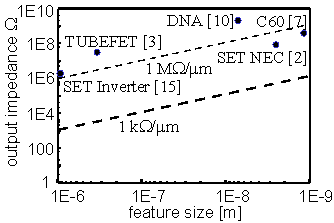
Fig. 5 The output impedance as a function of feature size. The general trend is that the output impedance increases as the size decreases.
6 Circuits
Not many circuits consisting of more than one single-electron transistor have been tested. A few simple memory and logic circuits have been fabricated using semiconductors and metal tunnel junctions. [11-14] No multiple transistor circuits have been made with carbon nanotubes. Metal tunnel junctions are currently the most mature technology for fabricating SET circuits. In this technology, wires can cross and transistors with voltage gain can be reproducibly fabricated. As an illustration of the present status of this technology, an inverter circuit is described below. [15]
Figure 6 shows a SEM photograph of a single-electron inverter that was fabricated using metal tunnel junctions. The inverter consists of two single-electron transistors in series that share a common input gate. The SET's are outlined with dotted lines in the schematic. For inverter operation, the output should be high when the input is low and the output should be low when the input is high. This is achieved by applying a bias voltage Vb and adjusting the two tuning gates such that when the input voltage is low, the top transistor is conducting and the bottom transistor is in Coulomb blockade. This effectively connects the output to the supply voltage and makes the output high. The Coulomb blockade prevents a steady current from flowing through the inverter limiting the dissipation in this device. When a high input voltage is applied, this shifts the induced charge on each of the SET's by a fraction of an electron and puts the top transistor in Coulomb blockade and makes the bottom transistor conducting so that the output is effectively connected to ground. Thus, when the input is high, the output is low. The measured inverter characteristics and simulations are shown in Fig. 7.
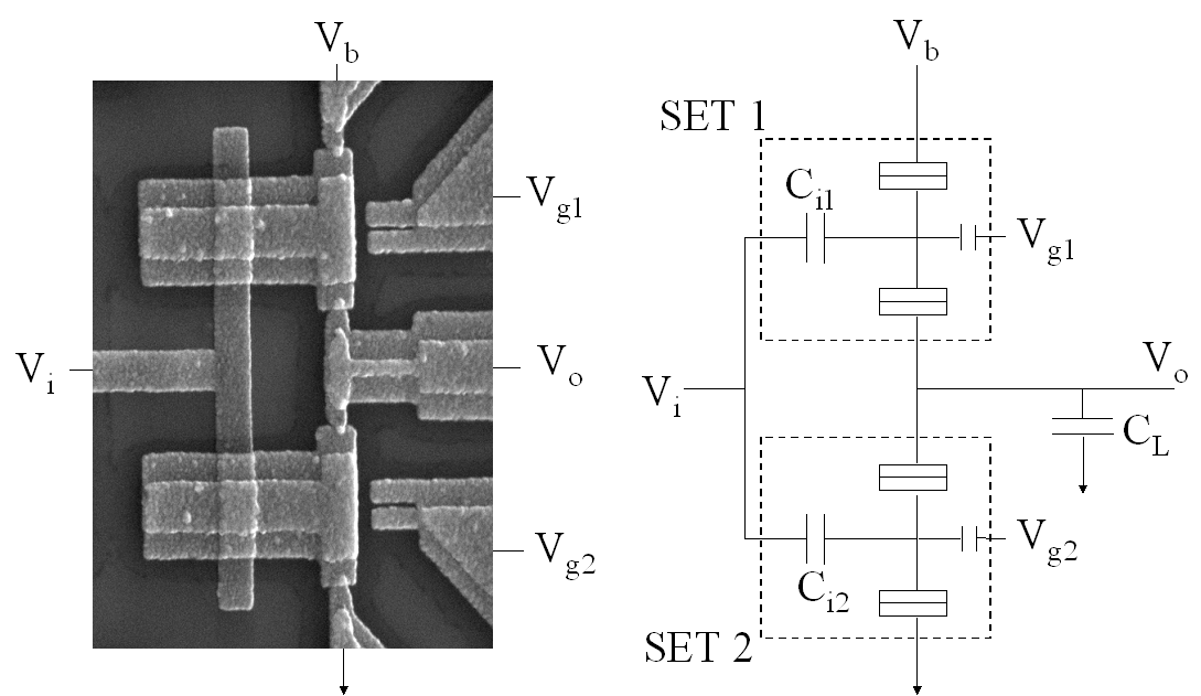
Fig. 6 On the left is a scanning electron microscope image of the inverter and on the right is the corresponding schematic. The width of the T-shaped islands is 1 mm. The dotted lines outline the two SET's in the circuit. The load capacitor CL is not shown in the SEM photo.
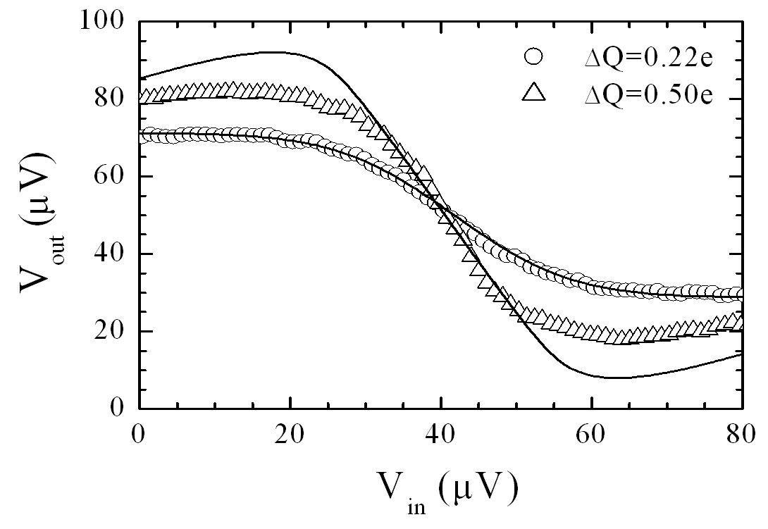
Fig. 7 The symbols are the measured input-output characteristics of the inverter. The solid lines are simulations based on the orthodox theory of single-electron tunneling.
An important consideration for the proper operation of an inverter is that the maximum output voltage swing must be greater than the voltage swing necessary at the input to switch the output from low to high. In other words, the inverter must exhibit voltage gain. The maximum voltage gain that can be achieved in a single-electron transistor is the ratio of the input-gate capacitance to the junction capacitance gv = Ci/Cj. In this circuit, overlap capacitors were used to make relatively large input-gate capacitors. The maximum voltage gain of the inverter, which can be determined from the slope of the transitional region in Fig. 7, was gv = 2.6. As the temperature was increased, the gain decreased. This inverter exhibited gain greater than one for temperatures up to 0.14 K. Fabricating a room-temperature single-electron transistor with voltage gain is much more challenging than making a room temperature SET that modulates the conductance at room temperature. The fabrication of a room temperature SET with gain almost certainly requires control of the fabrication process on a nanometer scale in three dimensions.
7 Fault tolerance
Single-electron transistors are sensitive to charges much smaller than the charge of an electron. Just a half of an electron can switch them from on to off. This makes them extremely sensitive to charged defects in the vicinity of such a transistor. A charged vacancy or an interstitial ion in the oxide of a single-electron transistor is enough to switch the transistor from on to off. When 100 SET's are fabricated, some of them will be switched on with zero voltage applied to the gate and some will be switched off with zero voltage applied to the gate. This is known as the background charge problem. During the course of time the charged defects often move or shift between two positions. These movements are detected by the single-electron transistors. The same kinds of charged defects are present and move in field-effect transistor circuits but field-effect transistors are not as sensitive to charge so the consequences of these background charges are not as great. The background charge problem makes it difficult to design robust circuits with single-electron transistors. Typically, the background charges have to be detected (one for every transistor in the circuit) and these charges have to be compensated for by applying additional voltages to the gates of the single-electron transistors.
8 Conclusions
The combination of large output impedance, low gain, and low fault tolerance conspire to make single-electron circuits non-competitive with field-effect transistors unless the SET's can be fabricated at a much higher device density than field-effect transistors. Voltage gain in room temperature single-electron transistors has not been demonstrated and will only be achieved when fabrication techniques have advanced so that three-dimensional structures can be made on the scale of a few nanometers. Until advances in the fabrication are made, single-electron transistors will be combined with field-effect transistors in applications where the superior charge sensitivity of the SET's can be used to advantage. In this case it is not important that the SET's display voltage gain. The field-effect transistors in the circuit can compensate for this.
8 Literature
[1] K. K. Likharev, Proceedings of the IEEE 87 p. 606, 1999
[2] Yu. A. Pashkin, Y. Nakamura, and J.S. Tsai, Appl. Phys. Lett. 76 p. 2256, 2000
[3] S.J. Tans, A.R.M. Verschueren, and C. Dekker Nature 393 p. 49-52, 1998
[4] Z. Yao, H.W.C. Postma, L. Balents and C. Dekker Nature 402 pp. 273-276 1999
[5] S. J. Tans, M. H. Devoret, R. J. A. Groeneveld, and C. Dekker, Nature 394 p. 761, 1998
[6] H. Postma, T. F. Teepen, and C. Dekker, to be published.
[7] H. Park, J. Park, A. K. L. Lim, E. H. Anderson, A. P. Alivisatos and P. L. McEuen, Nature 407, pp. 57 - 60, 2000
[8] The International Technology Roadmap for Semiconductors, http://public.itrs.net/files/1999_SIA_Roadmap/Home.htm
[9] F. G. Pikus and K. K. Likharev, Appl. Phys. Lett. 71 p. 3661, 1997
[10] Danny Porath, Alexy Bezryadin, Simon de Vries, and Cees Dekker Nature 403 p. 635, 2000
[11] Islamshah Amlani, Alexei O. Orlov, Ravi K. Kummamuru, Gary H. Bernstein, Craig S. Lent, and Gregory L. Snider,Applied Physics Letters, Vol. 77, No. 5, pp. 738–740, 2000
[12] Alexei O. Orlov, Islamshah Amlani, Ravi K. Kummamuru, Rajagopal Ramasubramaniam, Geza Toth, Craig S. Lent, Gary H. Bernstein, and Gregory L. Snider, Applied Physics Letters, Vol. 77, No. 2, pp. 295–297, 2000
[13] C. D. Chen; Y. Nakamura; T. S. Tsai, Applied-Physics-Letters. vol.71, p.2038-40, 1997
[14] C. P. Heij, D. C. Dixon, P. Hadley, and J. E. Mooij, Applied Physics Letters 74 p. 1042-1044, 1999
[15] A single-electron inverter C. P. Heij, P. Hadley, J. E. Mooij, to appear February 19, 2001 in Applied Physics Letters.