Jeong-O Lee,1* Günther Lientschnig,1 Frank Wiertz,1 Martin Struijk,2 Réne A. J. Janssen,2 Richard Egberink,3 David N. Reinhoudt,3 Andrew Grimsdale4, Klaus Müllen4, Peter Hadley,1 and Cees Dekker1
(1) Department of Nanoscience and DIMES, Delft University of Technology, Lorentzweg 1, 2628 CJ Delft, The Netherlands.
(2)Laboratory of Macromolecular and Organic Chemistry, Eindhoven University of Technology, P.O. Box 513, 5600 MB Eindhoven, The Netherlands.
(3) Laboratory for Supramolecular Chemistry and Technology, MESA+ Research Institute, University of Twente, P.O. Box 217, 7500 AE Enschede, The Netherlands.
(1)Synthetic Chemistry Group, Max Planck Institute for Polymer Research (MPIP), D55128 Mainz, Germany.
* Corresponding author: Jeong-O Lee, phone : +31-15-278-3552, fax : +31-15-278-1202, e mail : lee@mb.tn.tudelft.nl
Key Words; molecular electronics, conjugated molecules, transistor.
Abstract
We fabricated 3-terminal devices with conjugated molecules. Two different device layouts were used to measure both very short molecules (with one or two benzene rings) and relatively long ones (as long as 8 nm). To get an optimum gate effect, we used aluminum gates covered with a very thin natural aluminum oxide layer. Molecules with thiol end groups were positioned between the source and drain electrodes by self-assembly. The device yield was low for short molecules, most likely due to the defects in SAM. Most of the devices did not show any gate effect at all; a small gate effect was only observed in two samples made with 1,3-benzenedithiol. Some devices showed clear negative differential conductance peaks. In some devices made with long molecules, we observed a small change of conductance with gate voltage.
I. Introduction
As microelectronics evolves into nanoelectronics, chemical synthesis and self-assembly will be used more and more to fabricate electronic components. Chemically synthesized components can be atomically identical and cheaply manufactured. Because a single crystal substrate is not required, these devices can be used with inexpensive and flexible substrates. They are also suitable for three-dimensional integration since they can be grown or attached on top of previously deposited layers. This makes it interesting to characterize the electronic properties of a wide variety of molecules and self-assembled structures formed by molecules.
Here we examine the electronic transport through phenylene-based π-conjugated molecules. All of the measurements were made on parallel arrays of molecules in a three-terminal geometry where the molecules bridged two closely spaced metal electrodes and a nearby gate electrode was used to try to modulate the electronic levels of the molecules. Parallel arrays of molecules are interesting for many applications because they can have much lower resistances and can drive much more current than single molecules can. For the parallel arrays of molecules that were studied, we characterized the current stabilities, the field effect, the device-to-device reproducibility, and the long-term stability of the devices. Section II describes electronic transport measurements on self-assembled monolayers of short (~1 nm) phenylene-based π-conjugated molecules. These molecules are so short that little or no gate effects can be observed. Gate effects should be more pronounced for longer molecules. Section III describes the first measurements of a longer π-conjugated oligomer. This is about 8 nm long and a small reproducible gate effect was observed.
II. Short Molecules
Self-assembled monolayers (SAMs) of five small organic molecules were studied. These molecules are listed in Table I. The molecules were all phenylene-based conjugated oligomers consisting of one or two phenylene rings and end-capped with thiol groups or cyanide groups for stable contacts. The SAMs were sandwiched between two gold electrodes. Electronic transport was measured through the molecules while a voltage was applied to a nearby gate electrode. This geometry is referred to as a self-assembled monolayer field-effect transistor (SAMFET).
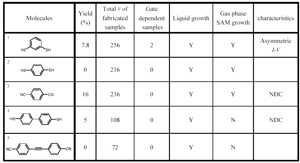
Table 1: Summary of the results from the fabrication and transport experiments on a variety of molecular devices. The molecules are 1: 1,3-benzenedithiol, 2: 1,4-benzenedithiol, 3: 1,4-phenylenediisocyanide, 4: 4,4´-biphenyldithiol, and 5: 4,4'-ethynediyl-di-benzonitrile. Molecules 1, 2, and 3 were purchased commercially from Aldrich chemicals and Tokyo Kasei respectively. Molecule 4 was synthesized for this work according to Ref. 10 by M. S., and 5 was synthesized for this work by R. E. As shown in the table, the yield of the devices was low, and gate dependences were observed only in 2 samples. A remarkable finding is that we obtained almost the same yield of devices for both vapor and liquid growth of SAMs for short molecules. NDC stands for the observation of negative differential conductance.
To make the devices, first a 30 nm thick aluminum gate electrode was fabricated on an oxidized silicon wafer using electron-beam lithography and lift-off. An aluminum oxide layer, a few nanometers thick, forms as soon as the aluminum is exposed to air. To get a smooth aluminum film and thereby a good quality oxide, the aluminum was evaporated at liquid nitrogen temperature. The next step in our fabrication scheme was to make a suspended bridge that was used as a deposition mask for the source and drain electrodes. We used a three-layer resist of either (from top to bottom) PMMA/Si/hard-baked-photoresist or PMMA/SiN/SiO2. A schematic diagram of the suspended resist bridge is shown in Fig. 1. Gold bottom electrodes were then evaporated at liquid nitrogen temperature at an angle of 10o to the surface normal. Measurements made between this gold electrode and the aluminum gate showed that there was no measurable leakage current for voltage differences up to about +/- 4 V. The chance of an aluminum oxide breakdown resulting in shorted electrodes strongly increased as the voltage was increased above 4 V. Such aluminum/aluminum-oxide gates have been shown to be able to produce a strong gating effect in molecular transistors.1-3
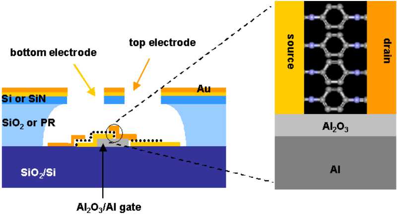
Figure 1: Schematic diagram of the device. The suspended bridge consists of hard baked photoresist or SiO2, and evaporated Si (or SiN).
Self-assembled monolayers of molecules were then grown on the bottom electrode by gas-phase deposition in a sealed container at 70oC for 24 hours in N2 atmosphere. Under such conditions, the thiol or cyanide-functionalized molecules assemble on the gold surface and form a highly ordered monolayer. We also grew SAMs in liquid to compare with gas phase deposition, and obtained a similar yield in both cases. In the final fabrication step, a gold top electrode was evaporated on top of the SAM. This evaporation was made at an angle of -10o at liquid nitrogen temperature using a very slow deposition rate (0.1 Ĺ/s) in order to avoid possible damage to the molecules. By adjusting the angle between the top electrode evaporation and the bottom electrode evaporation, it was possible to control the number of molecules that participate in transport.
As is shown in the Table 1, more than 1000 devices were fabricated. Many of them were electrically short circuited between source and drain electrodes. This can be attributed to imperfections in the SAMs that lead to shorts. All of the devices made from 1,4-benzenedithiol or biphenyldiisocyanide had shorts. We measured current-voltage characteristics and gate voltage dependences of the other three molecules: 1,3-benzenedithiol, 1,4-phenylenediisocyanide, and biphenyldithiol. Between 5% and 16% of the devices had resistances between 10 kΩ and 10 GΩ and there were large variations in the resistances in this range. The rest of the devices were either open circuited or shorted. The resistances generally increased with time becoming greater than 10 GΩ after two weeks. No discernable gate effect was observed in most of the devices, however, a weak gate effect was measured in two devices made using 1,3-benzenedithiol. For many samples, the electronic transport characteristics were irreproducible from measurement to measurement on the same sample. Below, we describe those measurements that were reproducible when the sample was repeatedly measured.
1,3-benzenedithiol
Figure 2(a) and (b) show the room temperature I-V curves for self-assembled monolayers of 1,3-benzenedithiol molecules at different gate voltages. The curves are asymmetric around the origin and the source-drain current slightly increases when a positive gate voltage is applied, indicating n-type behavior. The I-V curves increase exponentially in the positive bias region. Positive bias corresponds to electrons being emitted from the top electrode and collected at the bottom electrode.
Due to the very close spacing of the top and bottom electrodes (~1 nm), which is smaller than the thickness of the gate oxide, we would not expect a strong coupling of the gate to the molecules. From the geometry of the device, we estimate that only 0.5-3% of the contacted molecules would respond to the gate. The reason for the observed gate effect for these two devices is not clear.
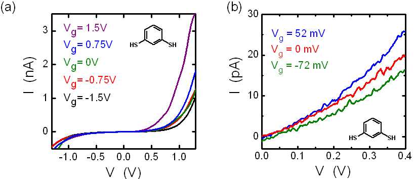
Figure 2: (a) I-V characteristics of a 1,3-benzenedithiol SAM between Au electrodes for various values of the gate voltage. Curves correspond to Vg=-1.5 V, -0.75 V, 0 V, 0.75 V, 1.5 V from the bottom to the top. (b) I-V characteristics of a 1,3-benzenedithiol SAM sandwiched between Pt electrodes. Due to a leakage current between Pt and Al/Al2O3 electrodes, only a limited range of gate voltage could be applied. Curves correspond to Vg=-72 mV, 0 V, 52 mV from the bottom to the top. All data were taken at room temperature.
1,4-phenylenediisocyanide
No reproducible gate effects were observed for devices fabricated with 1,4-phenylenediisocyanide. Figure 3(a) shows an I-V curve measured from the device fabricated with 1,4-phenylenediisocyanide at 4.2 K. We observe peaks in the differential conductance curve that are not due to switching events and a clear negative differential conductance at 350 mV. The sample shows a small amount of hysteresis between forward and backward sweeps. For all samples with 1,4-phenylenesiisocyanide, we observed unstable and noisy behavior at high voltage bias (> 1 V).
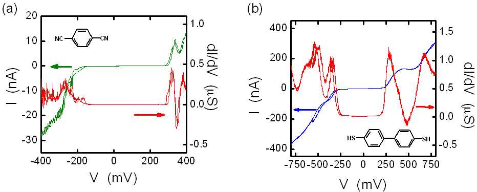
Figure 3: (a) I-V and dI/dV-V characteristics of a 1,4-phenylenediisocyanide sample with a small (~400 nm2) contact area. (b) I-V curve and dI/dV-V of biphenyldithiol. Both devices were measured at 4.2 K.
4,4´-biphenyldithiol
Figure 3(b) shows the measured characteristics for SAMs of biphenyldithiol. The I-V and dI/dV-V curves were measured simultaneously using a lock-in technique. No gate effects were observed in this system. The estimated contact area between source and drain was about 200 nm2. Two distinct peaks in the differential conductance were observed and a clear negative differential conductance region occurs at 460 mV. This may be explained by resonant tunneling through different molecular levels.4,5
The primary goal of this work was to understand the transport through self-assembled monolayers of short conjugated oligomers. We found large conductance fluctuations from sample to sample, which possibly may be understood as a strong sensitivity of the molecules to the contact configuration.6 We have also observed some interesting nonlinear transport characteristics for a small number of devices as well as a small gate effect for a few samples with 1,3-benzenedithiol SAMs. Overall, our measurements indicate that there is not much prospect for developing molecular electronics based on such SAMFETs.
Part of the motivation for studying these devices was to determine what truth there is in the recent publications of Schön et al.,7 on similar devices. Three of the molecules we studied, 1,4-phenylenediisocyanide, 1,4-benzenedithiol, and 4,4'-biphenyldithiol, also appear in the Schön publications. It is now understood that the Schön results are wrong8 and indeed we were not able to reproduce the good transistor characteristics that he reported. It is not surprising that these SAMFETs did not respond to the voltage applied to the gate. The source and drain contacts are so close together that they screen the molecules from the electric field generated by the gate. There is a rule of thumb in conventional silicon field-effect transistors that says that the source-drain separation should be about 45 times the gate oxide thickness.9 The source-drain distance in the SAMFETs is shorter than the gate oxide thickness. Stronger gate effects would be expected for longer molecules. In the next section, experiments are described using a fully conjugated organic molecule with a length of 8 nm.
III. Long Molecules
The long molecule that we studied, poly(dioctyloxybenzene) (AG180), is shown in the inset of Fig. 4. This molecule has side chains for solubility, and thio-methyl end-groups at both ends. To contact these molecules, three-terminal devices with gaps of less than 8 nm between the source and the drain electrodes were first fabricated. The same type of aluminum gate was used for these devices as for the short molecules. On top of the gate, gold electrodes with a thickness of 8 to 10 nm were evaporated and a gap of 8 nm was produced by shadow evaporation. Figure 4(a) shows a SEM image of the resulting structure after liftoff in warm acetone. Right after liftoff, the gold electrodes were checked on a probe station. A small fraction of the electrodes were shorted together. For all the other electrodes, no detectable current could be measured for bias voltages of up to 2 V.
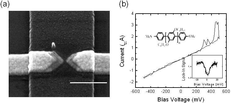
Figure 4: (a) Scanning electron microscope image of gold electrodes with a small gap on top of an Al/Al2O3 gate. The white scale bar is 300 nm. This particular device had a gap of 20 nm. (b) Differential conductance (dI/dV) measured with lock-in amplifier at 4.2 K. Inset shows the room temperature I-V curve of a device after having been subjected to a 0.1 mM AG180 chloroform solution. The molecular structure of AG180 is shown in the inset. For AG180, n is 18.
The samples were then put into a solution of chloroform at room temperature with 0.1 mM AG180 dissolved in it. After 24 to 48 hours, the samples were taken out of the solution, rinsed with chloroform to remove any physisorbed molecules, and checked again with the probe station. Some of the gold electrodes that did not show any conductance before now were clearly conducting, but with resistances varying in the range of a few hundred kΩ to several GΩ. As a control experiment, we put gap electrodes with similar gap sizes in a chloroform solution without AG180. None of the devices of this control experiment showed any conductance change. This strongly indicates that the measured currents were indeed carried by AG180 molecules.
The inset of Fig. 4(b) shows a typical current measurement taken at room temperature. The low resistance samples were quite unstable and showed a lot of switching noise. The devices that became conducting were bonded and measured again in a helium flow cryostat. Upon lowering the temperature, the resistance of the highly resistive (GΩ) samples increased drastically as the charge carriers froze out. The resistance of the low resistance (~300 kΩ) devices increased by a factor of 2 to 4. At low temperature and low bias voltages, the switching noise disappeared, and a small dip in the differential conductance was observed around zero bias with a gap size of about 10 mV. This can be seen in Fig. 4(b), which shows the differential conductance of a device that had a resistance of 1 MΩ at 4.2 K.
Figure 5(a) shows that the conductance between the source and the drain electrode is indeed slightly gate dependent. The change in source-drain current is shown as a function of gate voltage for a constant small bias voltage of 20 mV. At a gate voltage of 4 V, the change in current amounts to about 90 pA while the absolute current for these voltage conditions was 20 nA. The relative change in current was thus less than 0.5 percent. Figure 5(b) shows the conductance switching between two discrete states. This noisy behavior became more prominent for increased bias. Superimposed over the switching, the gate effect with a current change of about 340 pA can be seen. The relative gate effect for this bias voltage is about 0.3 percent, while the switching noise changes the current by 4 percent.
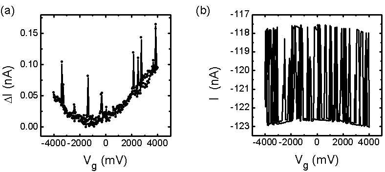
Figure 5: (a) The change in the current for a bias voltage of 20 mV as the gate voltage is swept from -4 to +4 V. The black, noisy curve was taken first, and the thick gray curve was taken after a 1 V sweep during which the resistance of the sample increased by a factor of 2. Nevertheless, the gate-induced change in current stayed the same, increasing the relative gate effect by 100%. (b) I-Vg curve measured at the high bias voltage (-100 mV). Conductance is switching between two discrete states.
It is striking that the long molecule sample has a relatively low resistance compared to the short molecule devices, although there are clearly far less molecules contacted in parallel. Due to the device geometry there is space for about 600 molecules contacted in parallel, but if we associate the switching noise in Fig. 5 (b) with a single molecule, then there would be only 25 molecules each with a resistance of 25 MΩ bound in parallel in this particular device. Because the molecule is bigger than those described in section II, one can imagine that the molecular orbitals are more closely spaced, forming bands along the molecule.
IV. Conclusions
In summary, we have studied the electrical transport properties of phenylene-based, π-conjugated molecules in a three-terminal geometry. In many cases, devices were short circuited between source and drain due to the imperfections in self-assembled monolayers. Due to the extremely short channel length compared with the gate oxide thickness, it is hard to expect a strong gate effect in such a system. Very small gate effects were observed in 2 samples out of 1000 devices tested. Our results show that it does not seem possible to realize field-effect transistors with the self-assembled monolayers of short phenylene-based molecules.
To improve the gate coupling, we fabricated devices with a longer (~8 nm) channel length. Long molecules with thio-methyl end-groups (AG180) were grown between source and drain electrodes patterned on top of Al/Al2O3 gates. We observed gate effects from the transistors fabricated with these long molecular wires, though the gate effect was very small. While the transistors we describe here do not seem promising for applications, the chemical route to the construction of electronic devices where molecules self-assemble into well defined structures seems so promising that we intend to pursue it further.
References
[1] Adrian Bachtold, Peter Hadley, Takechi Nakanishi and Cees Dekker, Science 294, 1317 (2001).
[2] N. B. Zhitenev, H. Meng, Z. Bao, Phys. Rev. Lett 88, 226801 (2002).
[3] Wenjie Liang, Matthew P. Shores, Marc Bockrath, Jeffrey R. Long and Hongkun Park, Nature, 417, 725-729 (2002).
[4] J. Chen, W. Wang, M. A. Reed, A. M. Rawlett, D. W. Price, and J. M. Tour, Appl. Phys. Lett, 77, 1224 (2000).
[5] Di Ventra, M., Pantelides, S. T. & Lang, N. D Appl. Phys. Lett, 76, 3448 (2000).
[6] J. Reichert, R. Ochs, D. Beckman, M. Mayor, H. v. Löhneysen, Phys. Rev. Lett 88, 176804-1 (2002).
[7] J. H. Schön, H. Meng, and Z. Bao, Nature (London) 413, 713 (2001).
[8] Beasley, M. R. (Chair); Datta, S.; Kogelnik, H.; Kroemer, H.; Monroe,D. Report of the investigation committee on the possibility of scientific misconduct in the work of Hendrik Schön and coauthors (September, 2002).
http://www.lucent.com/news_events/pdf/researchreview.pdf
[9] Scott Thompson, Paul Packan, and Mark Bohr, MOS Scaling: Transistor Challenges for the 21st Century, Intel Technology Journal Q3’98
[10] M. Rule, J. T. Tanner III, U. S. patent 5, 338, 886 (1994)