| JOURNAL OF LOW TEMPERATURE PHYSICS | Vol. 188, Nos. 5/6 | March 2000 |
Superconducting single-electron transistors (SSET's) are small islands of superconducting material isolated from an external circuit by tunnel barriers (Josephson junctions). The normal tunnel barrier resistances (R > h/4e2 ~ 6.5 kW) are sufficient to make the SSET's charge a good quantum number, so that the excess charge on the island is constrained to integer multiples of e. At equilibrium, adding an extra charge to the island costs a "charging energy" Ec = e2/2C, where C is the island's total capacitance.
At zero voltage bias, a supercurrent may flow coherently through the SSET, while for a large voltage bias (|eV| > 4D), the current is dominated by successive charging and discharging of the island by quasiparticles. Within a range of moderate bias (2D + Ec < |eV| < 2D + 3Ec), current flows via a hybrid transport mechanism termed the ''Josephson quasiparticle cycle'' (JQP). 1 In each turn of the cycle, a Cooper pair (CP) resonantly tunnels onto the SSET through one junction, followed by two successive quasiparticle (QP) tunneling events through the other junction, shuttling a charge of 2e between source and drain. The effective CP tunneling rate is typically slower than either QP tunneling rate, so the current is limited by the Josephson coupling.2
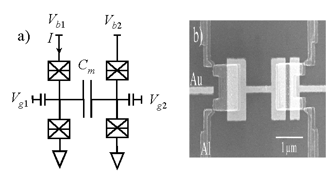
The SSET's were formed by the standard procedure of double angle evaporation of Al, with an oxidation step to form Al/AlOx tunnel barriers between each island and the leads. The gate electrodes and the central metal strip coupling the two islands were created in an underlying Au layer, with an intermediate insulation layer of SiO (32 nm). From normal-state measurements,3 the junction capacitances were seen to be in the 0.3 - 0.4 fF range, while Cm ~ 0.6 fF. The series resistances of the SSET's were 7 and 13 MW, so the Josephson energies of the tunnel junctions are expected to be very small (EJ < 0.1 meV) compared to the charging energy (Ec ~ 80 meV).
Measurements of the device were carried out at low electron temperature (27 mK) in a helium dilution refrigerator. The source-drain voltage biases for the two SSET's (Vb1, Vb2) were applied asymmetrically, with one lead from each SSET tied to ground. During our experiments, the left SSET was biased to the onset of JQP (eVb1 = 2D + Ec = 435 meV). When Vb2 was grounded, sweeping the gate voltage Vg1 produced a series of small peaks (~ 0.5 pA) periodic in gate charge of e (DVg1 = e/Cg1 ~ 3.8 mV).
The effects of biasing the other SSET are shown in Figure 2, where the current I is plotted as a function of Vg1, for various values of Vb2. Vg2was counterswept to cancel the cross-capacitance from the gate to the right SSET, fixing the induced charge of this SSET in each gate sweep. Capacitive effects due to the changing bias voltage were not cancelled, however, resulting in a slight leftward shift of the peaks for increasing Vb2.
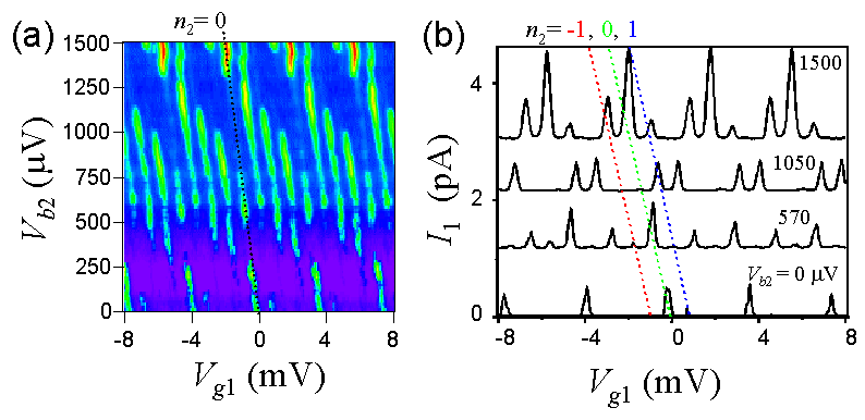
The increase in peak height is not presently understood, and in fact runs counter to expectations. Since JQP current is bottlenecked by the coherent CP tunneling step, it is hard to see how the stochastic fluctuations of n2 would increase this rate. Part of the explanation must take into account events involving the simultaneous transfer of charge in both SSET's. For example, a Cooper pair may tunnel into one of the SSET's while a quasiparticle tunnels out of the other SSET. However, preliminary calculations using the combined density matrix predict a suppression of the JQP current, not an enhancement, when the right SSET conducts a current of quasiparticles.