Problem 1
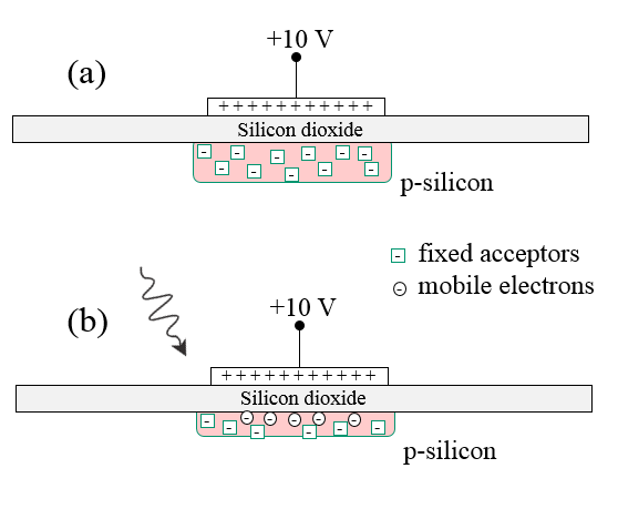
A positive voltage is applied to the gate of a MOS capacitor. This depletes the region under the gate as in figure (a).
(a) Draw the band diagram (conduction band, valence band, Fermi energy) along a line going from the metal across the oxide into the semiconductor. The p-type semiconductor is in depletion.
(b) Draw the electric field and the charge density.
(c) Light falls on this device and mobile electrons are collected at the silicon/oxide interface as in figure (b). Draw the electric field and the charge density for this situation.
Problem 2
(a) Draw an n-channel JFET.
(b) Explain how a JFET works.
(c) Where are there tunnel contacts in this device? What is the purpose of tunnel contacts? Draw the band diagram (valence band, conduction band, Fermi energy) of a tunnel contact.
(d) Why is a JFET slower than a MESFET?
Problem 3
(a) Draw an $n$-channel MOSFET showing the source, drain, gate, and body contacts.
(b) Draw the band diagram (conduction band, valence band, Fermi energy), and the electric field as a function of position in a MOS capacitor with a p-type substrate in accumulation.
(c) Consider a MOSFET in the linear regime (the gate is above the threshold to induce an inversion layer in the channel but the drain voltage is not so high as to cause pinch-off). How does the depletion width vary along the channel from source to drain?
(d) Explain what latch-up is in CMOS circuits.
Problem 4
(a) A $pnp$ bipolar transistor is constructed from GaAs, a direct bandgap semiconductor. When the emitter-base junction is forward biased, is light emitted like in a light emitting diode? Explain your reasoning.
(b) A JFET is constructed from GaAs. When the gate-channel junction is forward biased, is light emitted like in a light emitting diode? Explain your reasoning.
(c) A MESFET is constructed from GaAs. When the gate-channel junction is forward biased, is light emitted like in a light emitting diode? Explain your reasoning.