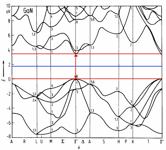
The band structure of a GaN is shown below. The zero of energy is chosen to be the top of the valence band.

(a) Is this a direct or an indirect semiconductor? Why? Solution
(b) What is the Fermi energy for GaN? Solution
(c) What is the band gap? Solution
(d) What are light holes and heavy holes? Explain how you can determine the effective mass of the holes from this diagram. Solution
(e) When is a semiconductor degenerately doped? Solution
The bottom of the conduction band is right above the top of the valence band in the $k$-space at $k=\Gamma$, therefore GaN is a direct semiconductor. The red lines in the annotated band diagram below mark the band edges and the bandgap.
The Fermi energy, which is at the blue line in the band diagram below, is about in the middle of the bandgap, which in case of GaN is at \[ \begin{equation} E_F=\frac{E_g}{2}=\frac{E_c-E_v}{2}=1.695\ eV \end{equation} \]

The bandgap of GaN is $E_g=\min(E_c)-\max(E_v)=3.4\ eV$.
Light and heavy hole bands are energy bands that converge at the valence band maximum. The light hole band is steeper than the heavy hole band. From \eqref{effmass} we can see that this results in a much lower effective mass of the holes. The holes in the heavy hole have a much higher effective mass and therefore dominate the properties of the semiconductor.
The effective mass of the holes can be determined by using the free electron approximation. That means the curvature of the valence band at the top is approximated by a parabola, allowing the use of the free electron model. The free electron energy is: \[ \begin{equation} E(k)=\frac{\hbar ^2k^2}{2m^*} \end{equation} \]
The effective mass can then be calculated by taking the second derivative of the energy with respect to $k$: \[ \begin{equation} \frac{d^2E(k)}{dk^2}=\frac{\hbar ^2}{m^*} \end{equation} \] \[ \begin{equation} \label{effmass} m^*=\frac{\hbar ^2}{\frac{d^2E(k)}{dk^2}} \end{equation} \]
Heavily doped semiconductors are called degenerately doped. When for n-type semiconductors $N_D \gt 0.1\ N_c$, then $E_F$ lies in the conduction band. Similarly for p-type semiconductors with $N_A \gt 0.1\ N_v$, $E_F$ lies in the valence band. In both cases, there is no bandgap anymore and the semiconductor starts to act like a metal.